

Fairchild Semiconductor SGP6N60UFD Datasheet
SGP6N60UFD
SGP6N60UFD
Ultra-Fast IGBT
General Description
Fairchild's UFD series of Insulated Gate Bipolar Transistors
(IGBTs) provides low conduction and switching losses.
The UFD series is designed for applications such as motor
control and general inverters where high speed switching is
a required feature.
Applications
AC & DC motor controls, general purpose inverters, robotics, and servo controls.
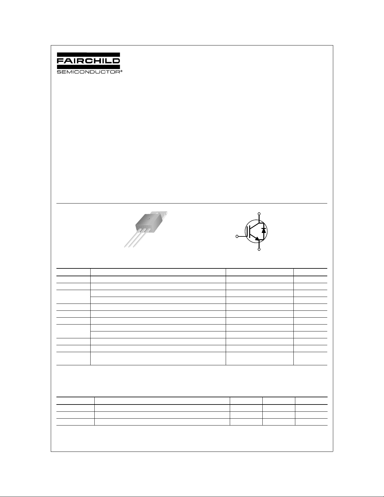
G C E
TO-220
Features
• High speed switching
• Low saturation voltage : V
• High input impedance
• CO-PAK, IGBT with FRD : t
= 2.1 V @ IC = 3A
CE(sat)
= 35ns (typ.)
rr
C
C
G
G
E
E
IGBT
Absolute Maximum Ratings T
Symbol Description SGP6N60UFD Units
V
CES
V
GES
I
C
I
CM (1)
I
F
I
FM
P
D
T
Operating Junction Temperature -55 to +150 °C
J
T
stg
T
L
Notes :
(1) Repetitive rating : Pulse width limited by max. junction temperature
Collector-Emitter Voltage 600 V
Gate-Emitter Voltage ± 20 V
Collector Current @ TC = 25°C6 A
Collector Current @ T
Pulsed Collector Current 25 A
Diode Continuous Forward Current @ TC = 100°C4 A
Diode Maximum Forward Current 25 A
Maximum Power Dissipation @ TC = 25°C30 W
Maximum Power Dissipation @ T
Storage Temperature Range -55 to +150 °C
Maximum Lead Temp. for Soldering
Purposes, 1/8” from Case for 5 Seconds
= 25°C unless otherwise noted
C
= 100°C3 A
C
= 100°C12 W
C
300 °C
Thermal Characteristics
Symbol Parameter Typ. Max. Units
R
(IGBT) Thermal Resistance, Junction-to-Case -- 4.0 °C/W
θJC
R
(DIODE) Thermal Resistance, Junction-to-Case -- 7.0 °C/W
θJC
R
θJA
Thermal Resistance, Junction-to-Ambient -- 62.5 °C/W
©2002 Fairchild Semiconductor Corporation SGP6N60UFD Rev. A1
SGP6N60UFD
Electrical Characteristics of the IGBT T
= 25°C unless otherwise noted
C
Symbol Parameter Test Conditions Min. Typ. Max. Units
Off Characteristics
BV
∆B
∆T
I
CES
I
GES
CES
VCES
J
Collector-Emitter Breakdown Voltage VGE = 0V, IC = 250uA 600 -- -- V
/
T emperature Coefficient of Breakdown
Voltage
Collector Cut-Off Current VCE = V
G-E Leakage Current VGE = V
V
= 0V, IC = 1mA -- 0.6 -- V/°C
GE
, VGE = 0V -- -- 250 uA
CES
, VCE = 0V -- -- ± 100 nA
GES
On Characteristics
V
GE(th)
V
CE(sat)
G-E Threshold Voltage IC = 3mA, VCE = V
,
Collector to Emitter
Saturation Voltage
= 3A
I
C
I
= 6A
C
VGE = 15V
,
VGE = 15V
GE
3.5 4.5 6.5 V
-- 2.1 2.6 V
-- 2.6 -- V
Dynamic Characteristics
C
ies
C
oes
C
res
Input Capacitance
Output Capacitance -- 22 -- pF
Reverse Transfer Capacitance -- 7 -- pF
= 30V, VGE = 0V,
V
CE
f = 1MHz
-- 220 -- pF
Switching Characteristics
t
d(on)
t
r
t
d(off)
t
f
E
on
E
off
E
Total Switching Loss -- 82 120 uJ
ts
t
d(on)
t
r
t
d(off)
t
f
E
on
E
off
Total Switching Loss -- 111 170 uJ
E
ts
Q
g
Q
ge
Q
gc
L
e
Turn-On Delay Time
-- 15 -- ns
Rise Time -- 25 -- ns
Turn-Off Delay Time -- 60 130 ns
Fall Time -- 70 150 ns
Turn-On Switching Loss -- 57 -- uJ
V
= 300 V, IC = 3A,
CC
R
= 80Ω, V
G
GE
Inductive Load, T
= 15V,
= 25°C
C
Turn-Off Switching Loss -- 25 -- uJ
Turn-On Delay Time
-- 22 -- ns
Rise Time -- 32 -- ns
Turn-Off Delay Time -- 80 200 n s
Fall Time -- 122 300 ns
Turn-On Switching Loss -- 65 -- uJ
= 300 V, IC = 3A,
V
CC
= 80Ω, V
R
G
GE
Inductive Load, T
= 15V,
= 125°C
C
Turn-Off Switchi ng Lo s s -- 46 -- uJ
Total Gate Charge
Gate-Emitter Charge -- 5 8 nC
Gate-Collector Charge -- 4 6 nC
= 300 V, IC = 3A,
V
CE
V
GE
= 15V
-- 15 22 nC
Internal Emitter Inductance Measured 5mm from PKG -- 7.5 -- nH
Electrical Characteristics of DIODE T
= 25°C unless otherwise noted
C
Symbol Parameter Test Conditions Min. Typ. Max. Units
T
V
FM
t
rr
I
rr
Q
rr
©2002 Fairchild Semiconductor Corporation
Diode Forward Voltage IF = 4A
Diode Reverse Recovery Time
Diode Peak Reverse Recovery
Current
Diode Reverse Recovery Charge
I
= 4A,
F
di/dt = 200A/us
= 25°C
C
= 100°C
T
C
TC = 25°C
= 100°C
T
C
T
= 25°C
C
= 100°C
T
C
T
= 25°C
C
= 100°C
T
C
-- 1.4 1.7
-- 1.3 --
-- 35 52
-- 53 --
-- 3.5 5.0
-- 4.5 --
-- 60 135
-- 120 --
V
ns
A
nC
SGP6N60UFD Rev. A1
SGP6N60UFD
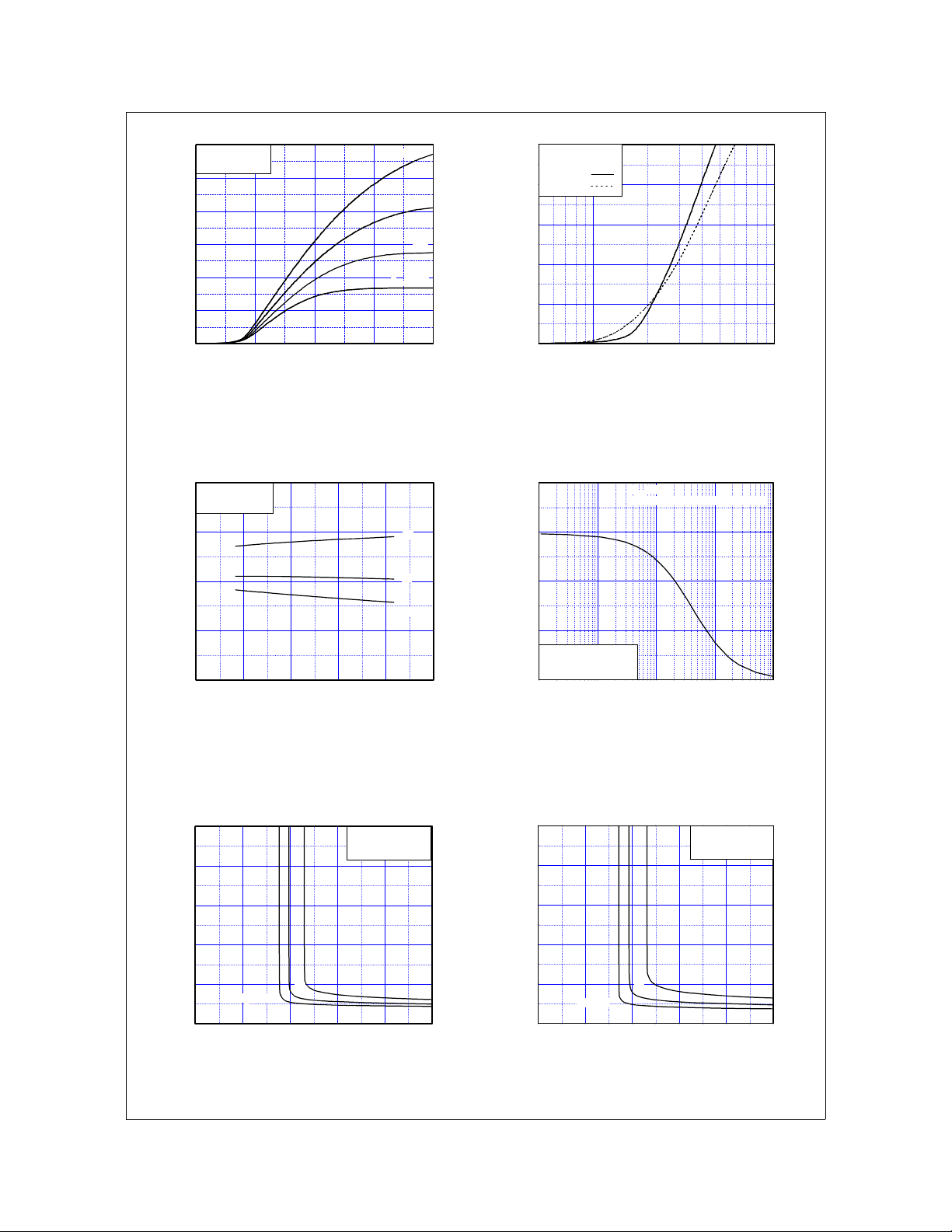
15
Common Emitter
V
= 15V
GE
= 25℃
T
C
12
T
= 125℃
C
[A]
C
9
6
Collector C urrent, I
3
0
0.5 1 10
Colle c tor - Emitte r V oltage, VCE [V]
[A]
C
30
Comm o n Emitt e r
TC = 25
25
20
15
10
℃
20V
15V
12V
VGE = 10V
Collector Current, I
5
0
02468
Collector - Emit ter Voltag e, VCE [V]
Fig 1. Typical Output Characteristics Fig 2. Typical Saturation Voltage
[V]
CE
4
Common E mitter
V
= 15V
GE
3
2
Characteristics
8
6A
3A
6
4
VCC = 300V
Load Current : peak of s qu are w ave
IC = 1.5A
1
Collector - Emitter Voltage, V
0
0306090120150
Case Temperature , TC [℃]
Fig 3. Saturation Voltage vs. Case
Temperature at Variant Current Level
20
16
[V]
CE
12
8
4
Collector - Emit t er Voltage, V
0
048121620
IC = 1.5A
3A
Gate - Emitter Voltage, VGE [V]
6A
Common Emitter
℃
T
= 25
C
Load Current [A]
2
Duty cycle : 50%
℃
= 100
T
C
Power Dissipation = 9W
0
0.1 1 10 100 1000
Frequency [KHz]
Fig 4. Load Current vs. Frequ ency
20
16
[V]
CE
12
8
4
Collector - Emitter Voltage, V
0
IC = 1.5A
0 4 8 12 16 20
3A
Gate - Emitter Voltage, VGE [V]
6A
Common Emitter
T
= 125
C
℃
Fig 5. Satur ation Voltage vs. V
©2002 Fairchild Semiconductor Corporation
Fig 6. Saturation Voltage vs. VGE
GE
SGP6N60UFD Rev. A1
 Loading...