

Fairchild Semiconductor SGF5N150UF Datasheet
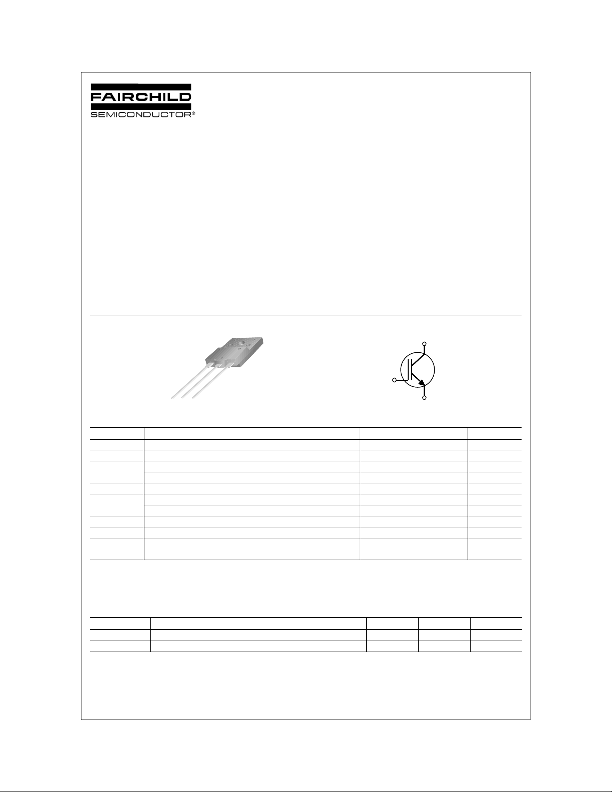
SGF5N150UF
IGBT
SGF5N150UF
General Description
Fairchild’s Insulated Gate Bipolar Transistor (IGBT)
provides low conduction and switching losses.
SGF5N150UF is designed for the Switching Power
Supply applications.
Application
Switching Power Supply - High Input Voltage Off-line Converter
F
3
P
O
T
C E
G
Absolute Maximum Ratings
Symbol Description SGF5N150UF Units
V
CES
V
GES
I
C
I
CM (1)
P
D
T
Operating Junction Temperature -55 to +150 °C
J
T
stg
T
L
Notes :
(1) Repetitive rating : Pulse width limited by max. junction temperature
Collector-Emitter Voltage 1500 V
Gate-Emitter Voltage ± 20 V
Collector Current @ TC = 25°C10 A
Collector Current @ T
Pulsed Collector Current 20 A
Maximum Power Dissipation @ TC = 25°C 62.5 W
Maximum Power Dissipation @ T
Storage Temperature Range -55 to +150 °C
Maximum Lead Temp. for Soldering
Purposes, 1/8” from Case for 5 Seconds
-
TC = 25°C unless otherwise noted
Features
• High Speed Switching
• Low Saturation Voltage : V
• High Input Impedance
G
G
= 100°C5 A
C
= 100°C25 W
C
300 °C
= 4.7 V @ IC = 5A
CE(sat)
C
C
E
E
Thermal Characteristics
Symbol Parameter Typ. Max. Units
R
θJC
R
θJA
©2003 Fairchild Semiconductor Corporation SGF5N150UF Rev. B
Thermal Resistance, Junction-to-Case -- 2.0 °C/W
Thermal Resistance, Junction-to-Ambient -- 40 °C/W
SGF5N150UF
Electrical Characteristics of IGBT
T
= 25°C unless otherwise noted
C
Symbol Parameter Test Conditions Min. Typ. Max. Units
Off Characteristics
BV
I
CES
I
GES
CES
Collector-Emitter Breakdown Voltage VGE = 0V, IC = 1mA 1500 -- -- V
Collector Cut-Off Current VCE = V
G-E Leakage Current VGE = V
, VGE = 0V -- -- 1.0 mA
CES
, VCE = 0V -- -- ± 100 nA
GES
On Characteristics
V
GE(th)
V
CE(sat)
G-E Threshold Voltage IC = 5mA, VCE = V
Collector to Emitter
Saturation Voltage
,
= 5A
C
VGE = 10V
I
GE
2.0 3.0 4.0 V
-- 4.7 5.5 V
Dynamic Characteristics
C
ies
C
oes
C
res
Input Capacitance
Output Capacitance -- 130 -- pF
Reverse Transfer Capacitance -- 70 -- pF
= 10V, VGE = 0V,
V
CE
f = 1MHz
-- 780 -- pF
Switching Characteristics
t
d(on)
t
r
t
d(off)
t
f
E
E
E
Q
Q
Q
on
off
ts
g
ge
gc
Turn-On Delay Time
= 600 V
V
Rise Time -- 15 -- ns
Turn-Off Delay Time -- 30 50 ns
Fall Time -- 70 120 ns
Turn-On Switching Loss -- 190 -- uJ
Turn-Off Switching Loss -- 100 -- uJ
Total Switching Loss -- 290 580 uJ
Total Gate Charge
Gate-Emitter Charge -- 3 5 nC
Gate-Collector Charge -- 15 25 nC
CC
= 5A
I
C
R
=10Ω
G
= 10V
V
GE
Inductive Load
T
C
V
V
= 25°C
= 600 V, IC = 5A
CE
GE
= 10V
-- 10 -- ns
-- 30 45 nC
©2003 Fairchild Semiconductor Corporation
SGF5N150UF Rev. B
 Loading...