

Fairchild Semiconductor SFR9220 Datasheet
Advanced Power MOSFET
SFR/U9220
FEATURES
Avalanche Rugged Technology
Rugged Gate Oxide Technology
Lower Input Capacitance
Improved Gate Charge
Extended Safe Operating Area
Lower Leakage Current : 10 µA (Max.) @ VDS = -200V
Lower R
: 1.111 Ω (Typ.)
DS(ON)
Absolute Maximum Ratings
Characteristic Value UnitsSymbol
Drain-to-Source Voltage
Continuous Drain Current (T
Continuous Drain Current (T
=25oC)
C
=100oC)
C
Drain Current-Pulsed
Gate-to-Source Voltage
Single Pulsed Avalanche Energy
Avalanche Current
Repetitive Avalanche Energy
Peak Diode Recovery dv/dt
Total Power Dissipation (T
Total Power Dissipation (T
=25oC)
A
=25oC)
C
*
Linear Derating Factor
Operating Junction and
Storage Temperature Range
Maximum Lead Temp. for Soldering
Purposes, 1/8“ from case for 5-seconds
T
V
DSS
I
I
DM
V
E
I
AR
E
dv/dt
P
, T
J
T
D
GS
AS
AR
D
STG
L
O
O
O
O
O
BV
R
I
1
1. Gate 2. Drain 3. Source
-200
-3.1
-1.96
1
2
1
1
3
-12
+
_
256
-3.1
3.0
-5.0
2.5
30
0.24
30
= -200 V
DSS
= 1.5 Ω
DS(on)
= -3.1 A
D
D-PAK
2
3
I-PAK
1
2
3
V
A
A
V
mJ
A
mJ
V/ns
W
W
W/
o
C
- 55 to +150
o
C
300
Thermal Resistance
Characteristic Max. UnitsSymbol Typ.
R
θJC
R
θJA
R
θJA
*
When mounted on the minimum pad size recommended (PCB Mount).
©1999 Fairchi ld Semiconduc tor Corpor ation
Junction-to-Case
Junction-to-Ambient
Junction-to-Ambient
*
--
--
--
4.17
50
110
o
C/W
Rev. B
SFR/U9220
P-CHANNEL
POWER MOSFET
Electrical Characteristics (T
CharacteristicSymbol
BV
∆BV/∆T
V
GS(th)
I
GSS
I
DSS
R
DS(on)
g
C
C
C
t
d(on)
t
d(off)
Q
Q
Q
Drain-Source Breakdown Voltage
DSS
Breakdown Voltage Temp. Coeff.
J
Gate Threshold Voltage
Gate-Source Leakage , Forward
Gate-Source Leakage , Reverse
Drain-to-Source Leakage Current
Static Drain-Source
On-State Resistance
Forward Transconductance
fs
Input Capacitance
iss
Output Capacitance
oss
Reverse Transfer Capacitance
rss
Turn-On Delay Time
t
Rise Time
r
Turn-Off Delay Time
t
Fall Time
f
Total Gate Charge
g
Gate-Source Charge
gs
Gate-Drain( “ Miller “ ) Charge
gd
=25oC unless otherwise specified)
C
Max. UnitsTyp.Min. Test Condition
V
-200
--
-2.0
--
--
--
--
--
--
--
--
--
--
--
--
--
--
--
--
--
-0.18
--
--
--
--
--
--
2.2
415
70
26
12
22
33
15
15
3.3
7.5
-4.0
-100
100
-100
--
--
-10
1.5
-540
105
40
35
55
75
40
19
--
--
V
GS
o
I
V/
nA
µA
nC
=-250µA See Fig 7
C
D
V
V
DS
V
GS
V
GS
V
DS
V
DS
V
Ω
GS
V
Ω
DS
V
GS
pF
ns
See Fig 5
V
DD
=18Ω
R
G
V
DS
I
=-3.5A
D
See Fig 6 & Fig 12
=0V,ID=-250µA
=-5V,ID=-250µA
=-30V
=30V
=-200V
=-160V,TC=125oC
=-10V,ID=-1.6A
=-40V,ID=-1.6A
O
O
4
4
=0V,VDS=-25V,f =1MHz
=-100V,ID=-3.5A,
See Fig 13
O
4
O
=-160V,VGS=-10V,
4
O
O
5
5
Source-Drain Diode Ratings and Characteristics
CharacteristicSymbol Max. UnitsTyp.Min. Test Condition
I
I
SM
V
t
Q
Notes ;
Repetitive Rating : Pulse Width Limited by Maximum Junction Temperature
1
O
2
L=40mH, I
O
3
I
O
SD
Pulse Test : Pulse Width = 250µs, Duty Cycle 2%
4
O
Essentially Independent of Operating Temperature
5
O
Continuous Source Current
S
Pulsed-Source Current
Diode Forward Voltage
SD
Reverse Recovery Time
rr
Reverse Recovery Charge
rr
=-3.1A, VDD=-50V, RG=27Ω*, Starting TJ =25oC
AS
_
-3.5A, di/dt 300A/µs, VDDBV
_
<
<
_
, Starting TJ =25oC
<
DSS
--
--
--
125
0.59
-3.1
-12
-5.0
--
--
--
1
--
O
4
--
O
--
--
_
<
Integral reverse pn-diode
A
in the MOSFET
V
T
=25oC,IS=-3.1A,VGS=0V
J
ns
T
=25oC,IF=-3.5A
J
µC
/dt=100A/µs
di
F
O
4
P-CHANNEL
POWER MOSFET
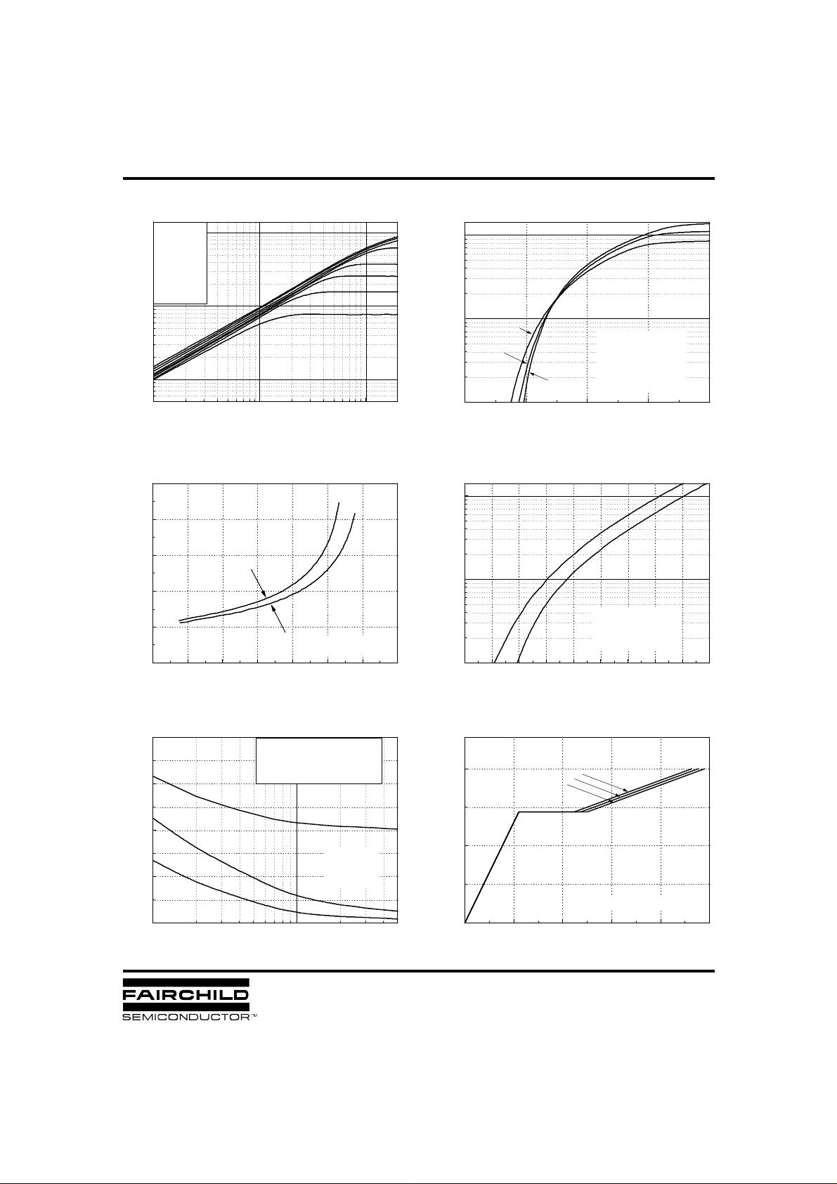
Fig 1. Output Characteristics Fig 2. Transfer Characteristics
V
1
10
0
10
, Drain Current [A]
D
-I
-1
10
10
5
4
]
Ω
, [
3
DS(on)
R
2
Drain-Source On-Resistance
1
0
GS
Top : - 15 V
- 10 V
- 8.0 V
- 7.0 V
- 6.0 V
- 5.5 V
- 5.0 V
Bottom : - 4.5 V
@ Notes :
s Pulse Test
1. 250
µ
= 25 oC
2. T
-1
C
0
10
-VDS , Drain-Source Voltage [V]
= -10 V
V
GS
VGS = -20 V
@ Note : TJ = 25 oC
0 2 4 6 8 10 12 14
-ID , Drain Current [A]
SFR/U9220
1
10
0
10
, Drain Current [A]
D
-I
-1
1
10
10
2 4 6 8 10
1
10
0
10
, Reverse Drain Current [A]
DR
-I
-1
10
0.5 1.0 1.5 2.0 2.5 3.0 3.5 4.0 4.5 5.0
o
C
150
25 oC
- 55
@ Notes :
= 0 V
1. V
GS
2. V
= -40 V
DS
3. 250
s Pulse Test
o
C
µ
-VGS , Gate-Source Voltage [V]
Fig 4. Source-Drain Diode Forward VoltageFig 3. On-Resistance vs. Drain Current
150 oC
o
25
C
, Source-Drain Voltage [V]
-V
SD
@ Notes :
1. V
2. 250
= 0 V
GS
s Pulse Test
µ
800
C
600
iss
400
C
oss
Capacitance [pF]
C
rss
200
0
0
10
-VDS , Drain-Source Voltage [V]
C
= Cgs+ Cgd ( Cds= shorted )
iss
C
= Cds+ C
oss
gd
C
= C
rss
gd
@ Notes :
1. V
2. f = 1 MHz
1
10
GS
= 0 V
Fig 6. Gate Charge vs. Gate-Source VoltageFig 5. Capacitance vs. Drain-Source Voltage
= -40 V
V
10
DS
= -100 V
V
DS
VDS = -160 V
5
, Gate-Source Voltage [V]
GS
-V
0
0 3 6 9 12 15
@ Notes : ID =-3.5 A
QG , Total Gate Charge [nC]
 Loading...