

Fairchild Semiconductor SFM9214 Datasheet
Advanced Power MOSFET
SFM9214
FEATURES
ν Avalanche Rugged Technology
ν Rugged Gate Oxide Technology
ν Lower Input Capacitance
ν Improved Gate Charge
ν Extended Safe Operating Area
ν Lower Leakage Current : 10 µA(Max.) @ V
ν Lower R
DS(ON)
: 3.5 Ω (Typ.)
Absolute Maximum Ratings
Characteristic Value UnitsSymbol
Drain-to-Source Voltage
Continuous Drain Current (T
Continuous Drain Current (T
=25oC)
A
=70oC)
A
Drain Current-Pulsed
Gate-to-Source Voltage
Single Pulsed Avalanche Energy
Avalanche Current
Repetitive Avalanche Energy
Peak Diode Recovery dv/dt
Total Power Dissipation (T
Linear Derating Factor
*
=25oC)
A
Operating Junction and
Storage Temperature Range
Maximum Lead Temp. for Soldering
Purposes, 1/8" from case for 5-seconds
T
V
I
V
E
I
E
dv/dt
P
, T
J
T
DSS
I
DM
AR
D
GS
AS
AR
D
STG
L
= -250V
DS
*
O
O
O
O
O
BV
R
DS(on)
DSS
= -250 V
= 4.0 Ω
ID= -0.45 A
SOT-223
2
1
3
1. Gate 2. Drain 3. Source
-250
-0.45
-0.3
1
2
1
1
3
-3.6
+
_
30
100
-0.45
0.16
-4.8
1.63
0.013
- 55 to +150
300
V
A
A
V
mJ
A
mJ
V/ns
W
W/
o
C
o
C
Thermal Resistance
Characteristic Max. UnitsSymbol Typ.
R
θJA
*
When mounted on the mi nimum pad size recommended (PCB Mount).
2001 Fairchild Semiconductor Corporation
Junction-to-Ambient
*
77--
o
C/W
Rev. B1
SFM9214
P-CHANNEL
POWER MOSFET
Electrical Characteristics
CharacteristicSymbol
BV
∆BV/∆T
V
GS(th)
I
GSS
I
DSS
R
DS(on)
g
C
C
C
t
d(on)
t
d(off)
Q
Q
Q
Drain-Source Breakdown Voltage
DSS
Breakdown Voltage Temp. Coeff.
J
Gate Threshold Voltage
Gate-Source Leakage , Forward
Gate-Source Leakage , Reverse
Drain-to-Source Leakage Current
Static Drain-Source
On-State Resistance
Forward Transconductance
fs
Input Capacitance
iss
Output Capacitance
oss
Reverse Transfer Capacitance
rss
Turn-On Delay Time
t
Rise Time
r
Turn-Off Delay Time
t
Fall Time
f
Total Gate Charge
g
Gate-Source Charge
gs
Gate-Drain(“Miller” ) Charge
gd
(TC=25
o
C unless otherwise specified)
Max. UnitsTyp.Min. Test Condition
V
V
--
--
-250
--
-2.0
--
--
--
--
--
--
--
--
--
--
--
--
--
--
--
--
-0.21
--
--
--
--
--
--
0.57
225
35
13
10
18
24
11
9
2.0
4.6
--
-4.0
-100
100
-10
-100
4.0
--
295
55
20
30
45
60
30
11
--
--
V/oC
GS
I
=-250µA See Fig 7
D
V
V
DS
V
GS
nA
V
GS
VDS=-250V
µA
V
DS
V
Ω
GS
S
V
DS
VGS=0V,VDS=-25V,f =1MHz
pF
VDD=-125V,ID=-1.6A,
R
ns
nC
=24Ω
G
V
DS
I
=-1.6A
D
See Fig 6 & Fig 12
=0V,ID=-250µA
=-5V,ID=-250µA
=-30V
=30V
=-200V,TC=125oC
=-10V,ID=-0.23A
=-40V,ID=-0.23A
See Fig 5
See Fig 13
O
=-200V,VGS=-10V,
O
4
O
4
O
4
5
O
4
5
O
Source-Drain Diode Ratings and Characteristics
CharacteristicSymbol Max. UnitsTyp.Min. Test Condition
I
I
SM
V
t
Q
Notes ;
Repetitive Rating : Pulse Wi dt h Limi ted by Maximum Junction Temperature
1
O
2
L=800mH, I
O
3
I
_
<
O
SD
4
Pulse Test : Pulse Width = 250µs, Duty Cycle 2%
O
Essentially Independent of Operating Temperature
5
O
Continuous Source Current
S
Pulsed-Source Current
Diode Forward Voltage
SD
Reverse Recovery Time
rr
Reverse Recovery Charge
rr
=-0.45A, VDD=-50V, RG=27Ω*, Starting TJ =25oC
AS
_
-1.6A, di/dt 250A/µs, VDDBV
<
, Starting TJ =25oC
_
<
DSS
-0.45
--
--
1
--
O
4
--
O
--
--
_
<
--
--
130
0.61
-3.6
-4.0
--
--
Integral reverse pn-diode
A
in the MOSFET
V
T
=25oC,IS=-0.45A,VGS=0V
J
ns
T
=25oC,IF=-1.6A
J
µC
di
/dt=100A/µs
F
O
4
P-CHANNEL
POWER MOSFET
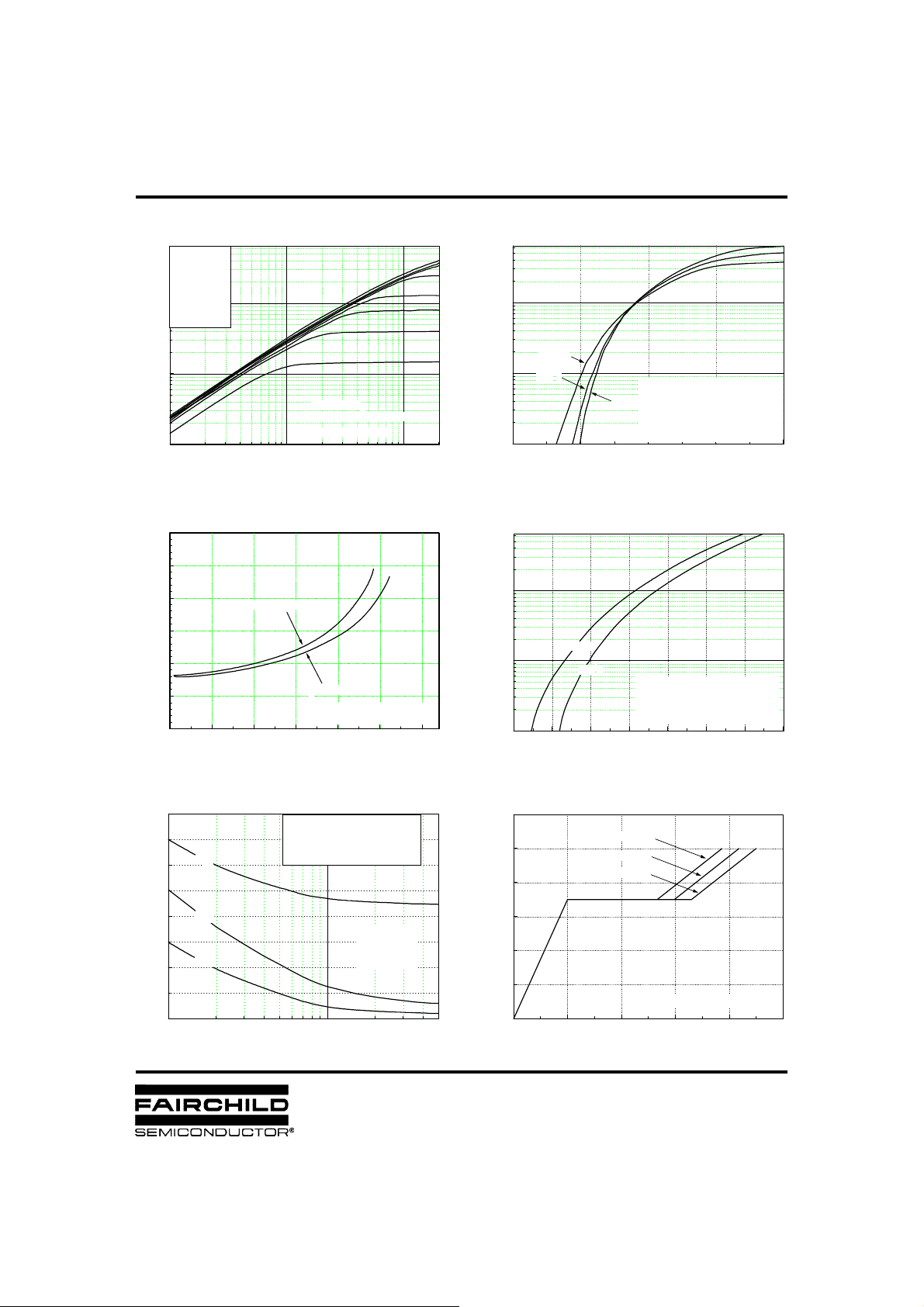
Fig 1. Output Characteristics Fig 2. Transfer Characteristics
V
GS
Top : -1 5 V
-10 V
-8.0 V
-7.0 V
-6.0 V
0
-5.5 V
10
-5.0 V
Botto m : -4.5 V
-1
10
, Drain Current [A]
D
-I
-2
10
-1
10
-VDS , Drain-Source Volt age [ V]
12
10
]
8
Ω
, [
6
DS(on)
R
4
VGS = -10 V
2
Drain-Source On -Resi sta nce
0
0123456
-ID , Drain Current [A]
@ Notes :
1. 250 µs Pulse Test
2. TC = 25 oC
0
10
VGS = -20 V
@ Note : TJ = 25 oC
SFM9214
0
10
150 oC
-1
10
25 oC
@ Notes :
, Drain Current [A]
D
- 55 oC
-I
-2
1
10
10
246810
-VGS , Gate-Source Voltage [V]
Fig 4. Source-Drain Diode Forward VoltageFig 3. On-Resistance vs. Drain Current
0
10
-1
10
, Reverse Drain Cu rrent [A]
DR
-2
-I
10
0.5 1.0 1.5 2.0 2.5 3. 0 3.5 4.0
150 oC
25 oC
-VSD , Source-Drain Vol tage [ V]
1. V
GS
2. V
DS
3. 250
@ Notes :
1. V
GS
2. 250
= 0 V
= -40 V
µ
s Pulse Test
= 0 V
µ
s Pulse Test
400
C
300
200
Capacitance [pF]
100
iss
C
oss
C
rss
0
0
10
C
= Cgs+ Cgd ( Cds= shorted )
iss
= Cds+ C
C
oss
gd
C
= C
rss
gd
@ Notes :
1. V
2. f = 1 MHz
1
10
GS
= 0 V
-VDS , Drain-Source Voltage [V]
12
VDS = -50 V
10
8
VDS = -125 V
VDS = -200 V
6
4
2
, Gate-Source Volt age [V]
GS
0
0246810
-V
QG , Total Gate Charg e [nC]
@ Notes : ID = -1.6 A
Fig 6. Gate Charge vs. Gate-Source VoltageFig 5. Capacitance vs. Drain-Source Voltage
 Loading...