

Fairchild Semiconductor RM4558D, RM4558D-883B Datasheet
www.fairchildsemi.com
Features
• 2.5 MHz unity gain bandwidth
• Supply voltage ±22V for RM4558 and ±18V for
RC/RV4558
• Short-circuit protection
• No frequency compensation required
Description
The RC4558 integrated circuit is a dual high-gain operational amplifier internally compensated and constructed on a
single silicon IC using an advanced epitaxial process.
Combining the features of the 741 with the close parameter
matching and tracking of a dual device on a monolithic chip
results in unique performance characteristics. Excellent
channel separation allows the use of this dual device in dense
single 741 operational amplifier applications. It is especially
well suited for applications in differential-in, differential-out
as well as in potentiometric amplifiers and where gain and
phase matched channels are mandatory.
• No latch-up
• Large common-mode and differential voltage ranges
• Low power consumption
• Parameter tracking over temperature range
• Gain and phase match between amplifiers
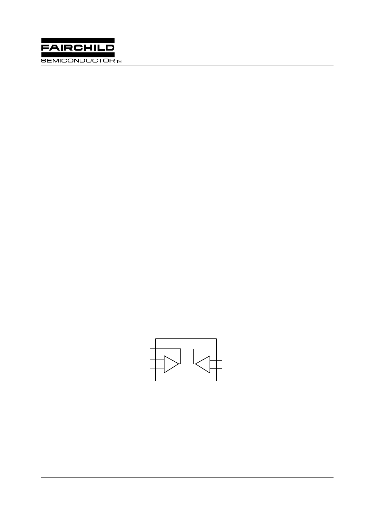
Block Diagram
65-4558-01
A
Output (A)
–Input (A)
–Input (A)
Output (B)
–Input (B)
+Input (B)
B
+
_
+
_
RC4558
Dual High-Gain Operational Amplifier
Rev. 1.0.0
PRODUCT SPECIFICATION RC4558
2
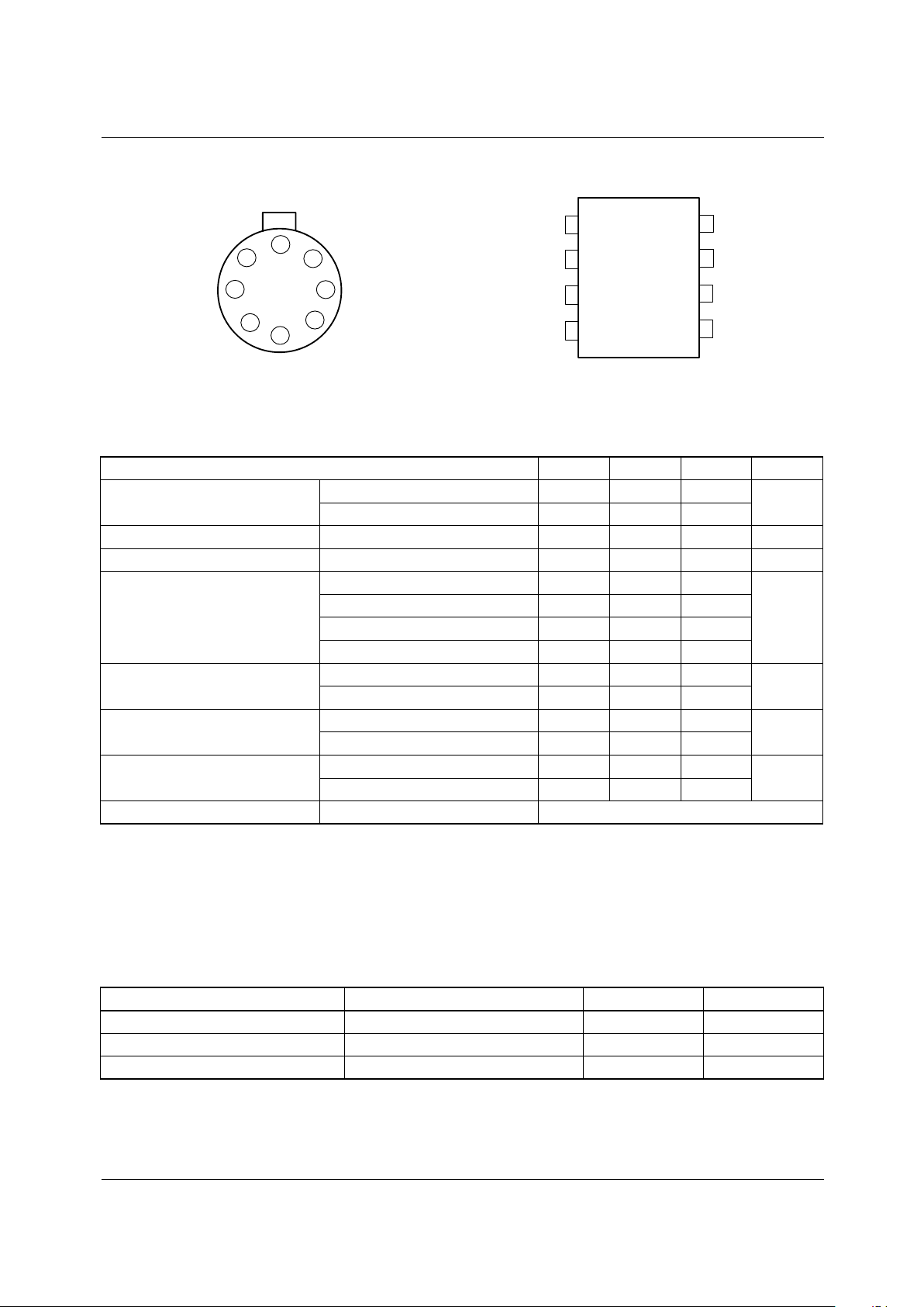
Pin Assignments
Absolute Maximum Ratings
(beyond which the device may be damaged)
1
Notes:
1. Functional operation under any of these conditions is NOT implied.
2. For supply voltages less than ±15V, the absolute maximum input voltage is equal to the supply voltage.
3. Short circuit may be to ground on one op amp only. Rating applies to +75°C ambient temperature.
Matching Characteristics
(VS = ±15V, TA = +25°C unless otherwise specified)
Parameter Min Typ Max Units
Supply Voltage RM4558 ±22 V
RC4558 ±18
Input Voltage
2
±15 V
Differential Input Voltage 30 V
PDTA < 50°C SOIC 300 mW
PDIP 468
CerDIP 833
TO-99 658
Junction Temperature SOIC, PDIP 125 °C
CerDIP, TO-99 175
Operating Temperature RM4558 -55 125 °C
RC4558 0 70
Lead Soldering Temperature PDIP, CerDIP, TO-99 (60 sec) 300 °C
SOIC (10 sec) 260
Output Short Circuit Duration
3
Indefinite
Parameter Test Conditions Typ Units
Voltage Gain RL ³ 2 kW±1.0 dB
Input Bias Current RL ³ 2 kW±15 nA
Input Offset Current RL ³ 2 kW±7.5 nA
1
2
3
4
5
6
7
8
65-3473-02
Output (A)
–Input (A)
+Input (A)
Output (B)
–Input (B)
+Input (B)
–V
S
+V
S
Output (A)
–Input (A)
+Input (A)
–V
S
+V
S
Output (B)
–Input (B)
+Input (B)
1
2
3
4
8
7
6
5
65-3473-03
RC4558 PRODUCT SPECIFICATION
3
Electrical Characteristics
(VS = ±15V and TA = +25°C unless otherwise specified)
The following specifications apply for RM = -55°C £ T
A
£ +125°C, RC = 0° £ TA £ +70°C
RM4558 RC4558
Parameters Test Conditions Min Typ Max Min Typ Max Units
Input Offset Voltage R
S
£ 10kW 1.0 5.0 2.0 6.0 mV
Input Offset Current 5.0 200 5.0 200 nA
Input Bias Current 40 500 40 500 nA
Input Resistance 0.3 1.0 0.3 1.0 MW
Large Signal Voltage Gain RL ³ 2kW, V
OUT
= ±10V 50 300 20 300 V/mV
Output Voltage Swing R
L
³ 10kW±12 ±14 ±12 ±14 V
RL ³ 2kW±10 ±13 ±10 ±13 V
Input Voltage Range ±12 ±13 ±12 ±13 V
Common Mode Rejection Ratio RS £ 10kW 70 100 70 100 dB
Power Supply Rejection Ratio RS £ 10kW 76 100 76 100 dB
Power Consumption RL = ¥ 100 170 100 170 mW
Transient Response VIN = 20 mV
Rise Time RL = 2kW 0.3 0.3 mS
Overshoot CL £ 100pF 35 35 %
Slew Rate R
L
³ 2kW 0.8 0.8 V/mS
Channel Separation F = 10kHz, RS = 1kW 90 90 dB
Unity Gain Bandwidth (Gain = 1) 2.5 3.0 2.0 3.0 MHz
Parameters Test Conditions
RM4558 RC4558
Min Typ Max Min Typ Max Units
Input Offset Voltage R
S
£ 10kW 6.0 7.5 mV
Input Offset Current
RC4558 500 300 nA
Input bias Current
RC4558 1500 800 nA
Large Signal Voltage Gain RL ³ 2kW, V
OUT
= ±10 25 15 V/mV
Output Voltage Swing RL ³ 2kW±10 ±10 V
Power Consumption RL = ¥ 120 200 120 200 mW
 Loading...