

Fairchild Semiconductor RFP22N10 Datasheet
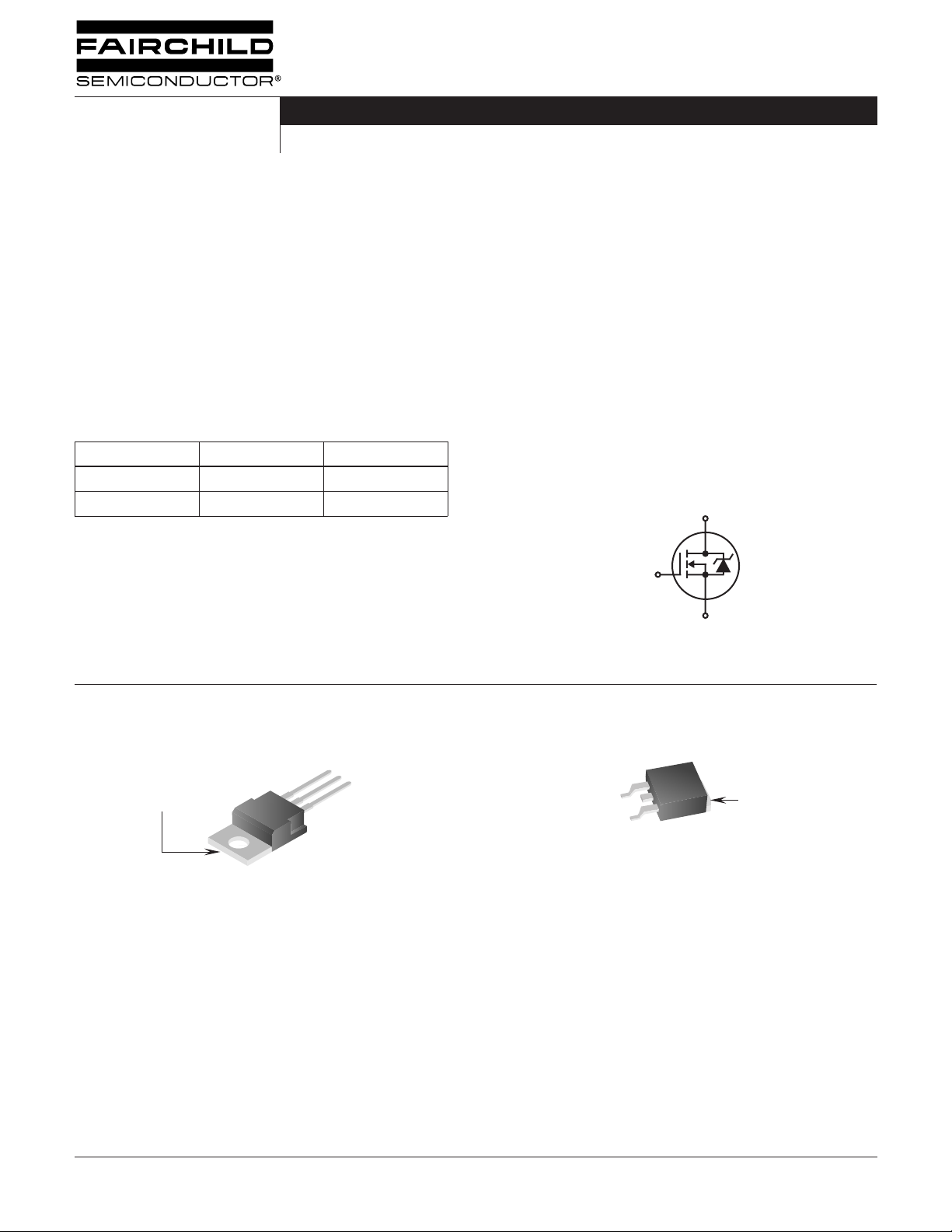
D
G
S
DRAIN
(FLANGE)
GATE
SOURCE
RFP22N10, RF1S22N10SM
Data Sheet January 2002 File Number 2385.3
22A, 100V, 0.080 Ohm, N-Channel Power
MOSFETs
These N-Channel power MOSFETs are manufactured using
the MegaFET process. This process, which uses feature
sizes approaching those of LSI integrated circuits gives
optimum utilization of silicon, resulting in outstanding
performance. They were designed for use in applications
such as switching regulators, switching converters, motor
drivers, and relay drivers. These transistors can be operated
directly from integrated circuits.
Formerly developmental type TA9845.
Ordering Information
PART NUMBER PACKAGE BRAND
RFP22N10 TO-220AB RFP22N10
RF1S22N10SM TO-263AB F1S22N10
NOTE: When ordering use the entire part number. Add the suffix, 9A,
to obtain the TO-263AB variant in tape and reel, e.g. RF1S22N10SM9A.
Features
• 22A, 100V
•r
DS(ON)
• UIS SOA Rating Curve (Single Pulse)
• SOA is Power Dissipation Limited
• Nanosecond Switching Speeds
• Linear Transfer Characteristics
• High Input Impedance
• 175
• Related Literature
- TB334 “Guidelines for Soldering Surface Mount
= 0.080 Ω
o
C Operating Temperature
Components to PC Boards”
Symbol
Packaging
JEDEC TO-220AB JEDEC TO-263AB
SOURCE
DRAIN
DRAIN
(FLANGE)
©2002 Fairchild Semiconductor Corporation RFP22N10, RF1S22N10SM Rev. B
GATE
±
µ
µ
±
Ω
≈
θ
θ
RFP22N10, RF1S22N10SM
Absolute Maximum Ratings
o
T
= 25
C, Unless Otherwise Specified
C
RFP22N10,
RF1S22N10SMS UNITS
Drain to Source Voltage (Note 1) . . . . . . . . . . . . . . . . . . . . . . . . . . . . . . . . . . . . . . . . . . . . . V
Drain to Gate Voltage (R
= 1M Ω ) (Note 1) . . . . . . . . . . . . . . . . . . . . . . . . . . . . . . . . . . .V
GS
Gate to Source Voltage . . . . . . . . . . . . . . . . . . . . . . . . . . . . . . . . . . . . . . . . . . . . . . . . . . . . .V
Continuous Drain Current . . . . . . . . . . . . . . . . . . . . . . . . . . . . . . . . . . . . . . . . . . . . . . . . . . . . .I
Pulsed Drain Current . . . . . . . . . . . . . . . . . . . . . . . . . . . . . . . . . . . . . . . . . . . . . . . . . . . . . . . I
Maximum Power Dissipation . . . . . . . . . . . . . . . . . . . . . . . . . . . . . . . . . . . . . . . . . . . . . . . . . . P
DSS
DGR
GS
D
DM
D
Linear Derating Factor . . . . . . . . . . . . . . . . . . . . . . . . . . . . . . . . . . . . . . . . . . . . . . . . . . . . . . . 0.67 W/
Operating and Storage Temperature . . . . . . . . . . . . . . . . . . . . . . . . . . . . . . . . . . . . . . . T
, T
J
STG
Maximum Temperature for Soldering
Leads at 0.063in (1.6mm) from Case for 10s. . . . . . . . . . . . . . . . . . . . . . . . . . . . . . . . . . . . T
Package Body for 10s, See Techbrief 334 . . . . . . . . . . . . . . . . . . . . . . . . . . . . . . . . . . . . .T
CAUTION: Stresses above those listed in “Absolute Maximum Ratings” may cause permanent damage to the device. This is a stress only rating and operation of the
device at these or any other conditions above those indicated in the operational sections of this specification is not implied.
L
pkg
100 V
100 V
20 V
22
50
100 W
-55 to 175
300
260
A
A
o
C
o
C
o
C
o
C
NOTE:
J
= 25
o
C to 150
1. T
Electrical Specifications
o
C.
o
T
= 25
C, Unless Otherwise Specified
C
PARAMETER SYMBOL TEST CONDITIONS MIN TYP MAX UNITS
Drain to Source Breakdown Voltage BV
Gate to Source Threshold Voltage V
GS(TH)
Zero-Gate Voltage Drain Current I
Gate to Source Leakage Current I
Drain to Source On Resistance (Note 2) r
DS(ON)
Turn-On Time t
Turn-On Delay Time t
d(ON)
Rise Time t
Turn-Off Delay Time t
d(OFF)
Fall Time t
Turn-Off Time t
Total Gate Charge Q
(OFF)
G(TOT)
Gate Charge at 10V Q
Threshold Gate Charge Q
Thermal Resistance Junction to Case R
Thermal Resistance Junction to Ambient R
DSS
GSS
(ON)
G(10)
G(TH)
I
DSS
r
= 250 µ A, V
D
V
= V
GS
DS
V
= 80V, V
DS
V
= 80V, V
DS
V
= ± 20V, V
GS
I
= 22A, V
D
V
= 50Vwwwwwwwww, I
DD
R
= 4.5 Ω , V
L
R
= 25 Ω
GS
(Figure 11)
= 0 (Figure 7) 100 - - V
GS
, I
= 250 µ A (Figure 9) 2 - 4 V
D
= 0V - - 1
GS
= 0V, T
GS
= 0 - -
DS
= 10V (Figure 8) - - 0.080
GS
= 10V,
GS
= 150
C
o
C--50
= 11A,
D
- - 60 ns
-13-ns
-24-ns
-65-ns
f
-18-ns
- - 120 ns
V
= 0V to 20V V
GS
V
= 0V to 10V - - 75 nC
GS
V
= 0V to 2V - - 3.5 nC
GS
JC
TO-220 and TO-263 - - 62
JA
= 80V, I
DD
R
= 3.64 Ω
L
I
= 1mA
g(REF)
(Figure 11)
22A,
D
- - 150 nC
- - 1.5
100 nA
o
C/W
o
C/W
A
A
Source to Drain Diode Specifications
PARAMETER SYMBOL TEST CONDITIONS MIN TYP MAX UNITS
Source to Drain Diode Voltage (Note 2) V
Diode Reverse Recovery Time t
NOTE:
2. Pulse Test: Pulse Duration = 300 µ s maximum, duty cycle = 2%.
©2002 Fairchild Semiconductor Corporation RFP22N10, RF1S22N10SM Rev. B
SD
rr
I
= 22A - - 1.5 V
SD
I
= 22A, dI
SD
/dt = 100A/ µ s - - 200 ns
SD
 Loading...