

Fairchild Semiconductor RFP15N05L Datasheet
RFP15N05L, RFP15N06L
Data Sheet January 2002
15A, 50V and 60V, 0.140 Ohm, Logic Level
N-Channel Power MOSFETs
These are N-Channel enhancement mode silicon gate
power field effect transistors designed for applications such
as switching regulators, switching converters, motor drivers,
relay drivers and drivers for high power bipolar switching
transistors requiring high speed and low gate drive power.
These types can be operated directly from integrated
circuits.
Formerly developmental type TA0522.
Ordering Information
PART NUMBER PACKAGE BRAND
RFP15N05L TO-220AB RFP15N05L
RFP15N06L TO-220AB RFP15N06L
NOTE: When ordering, use the entire part number.
Features
• 15A, 50V and 60V
•r
• Design Optimized for 5V Gate Drives
• Can be Driven from QMOS, NMOS, TTL Circuits
• Compatible with Automotive Drive Requirements
• SOA is Power Dissipation Limited
• Nanosecond Switching Speeds
• Linear Transfer Characteristics
• High Input Impedance
• Majority Carrier Device
• Related Literature
- TB334 “Guidelines for Soldering Surface Mount
= 0.140 Ω
DS(ON)
Components to PC Boards”
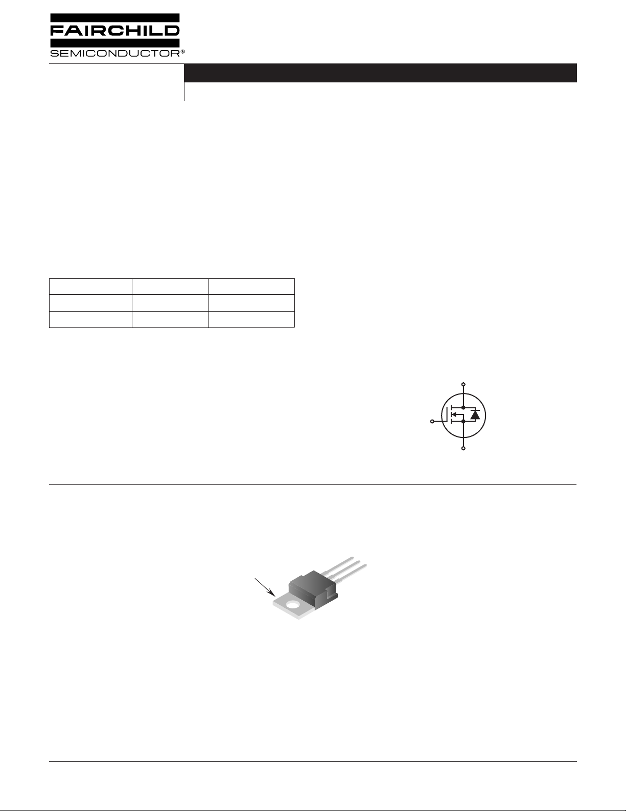
Symbol
D
Packaging
DRAIN
(TAB)
JEDEC TO-220AB
SOURCE
DRAIN
GATE
G
S
©2002 Fairchild Semiconductor Corporation RFP15N05L, RFP15N06L Rev. B
± 10 ±
µ
θ
RFP15N05L, RFP15N06L
Absolute Maximum Ratings
o
T
= 25
C, Unless Otherwise Specified
C
RFP15N05L RFP15N06L UNITS
Drain to Source Voltage (Note 1) . . . . . . . . . . . . . . . . . . . . . . . . . . . . . . . . . . . . . . . . . . . . . . . V
Drain to Gate Voltage (R
= 20k Ω) (Note 1) . . . . . . . . . . . . . . . . . . . . . . . . . . . . . . . . . . . . . V
GS
Continuous Drain Current . . . . . . . . . . . . . . . . . . . . . . . . . . . . . . . . . . . . . . . . . . . . . . . . . . . . . . . I
Pulsed Drain Current (Note 3) . . . . . . . . . . . . . . . . . . . . . . . . . . . . . . . . . . . . . . . . . . . . . . . . . I
Gate to Source Voltage . . . . . . . . . . . . . . . . . . . . . . . . . . . . . . . . . . . . . . . . . . . . . . . . . . . . . . . V
Maximum Power Dissipation . . . . . . . . . . . . . . . . . . . . . . . . . . . . . . . . . . . . . . . . . . . . . . . . . . . . P
Above T
o
= 25
C, Derate Linearly . . . . . . . . . . . . . . . . . . . . . . . . . . . . . . . . . . . . . . . . . . . . . . . . .
C
Operating and Storage Temperature . . . . . . . . . . . . . . . . . . . . . . . . . . . . . . . . . . . . . . . . . . T
DSS
DGR
D
DM
GS
D
T
J,
STG
Maximum Temperature for Soldering
Leads at 0.063in (1.6mm) from Case for 10s. . . . . . . . . . . . . . . . . . . . . . . . . . . . . . . . . . . . . . . T
Package Body for 10s, See Techbrief 334 . . . . . . . . . . . . . . . . . . . . . . . . . . . . . . . . . . . . . . . T
CAUTION: Stresses above those listed in “Absolute Maximum Ratings” may cause permanent damage to the device. This is a stress only rating and operation of the
device at these or any other conditions above those indicated in the operational sections of this specification is not implied.
L
pkg
50 60 V
50 60 V
15
40
15
40
10 V
60
0.48
60
0.48
-55 to 150 -55 to 150
300
260
300
260
W/
A
A
W
o
C
o
C
o
C
o
C
NOTE:
J
= 25
o
C to 125
1. T
Electrical Specifications
o
C.
o
T
= 25
C, Unless Otherwise Specified
C
PARAMETER SYMBOL TEST CONDITIONS MIN TYP MAX UNITS
Drain to Source Breakdown Voltage BV
DSS
I
= 250 µ A, V
D
GS
= 0V
RFP15N05L 50 - - V
RFP15N06L 60 - - V
Gate Threshold Voltage V
Zero Gate Voltage Drain Current I
Gate to Source Leakage Current I
Drain to Source On Resistance (Note 2) r
DS(ON)
Input Capacitance C
Output Capacitance C
Reverse-Transfer Capacitance C
Turn-On Delay Time t
GS(TH)
DSS
GSS
ISS
OSS
RSS
d(ON)
V
= V
GS
V
= 48V, V
DS
V
= 48V, V
DS
V
= ± 10V, V
GS
I
= 15A, V
D
V
= 25V, V
DS
(Figure 8)
V
= 30V, I
DD
, I
= 250 µ A (Figure 7) 1 - 2 V
DS
D
= 50V - - 1
DS
= 50V TC = 125
DS
= 0V - - 100 nA
DS
= 5V (Figures 5, 6) - - 0.140 Ω
GS
= 0V, f = 1MHz
GS
o
C--50 µ A
- - 900 pF
- - 450 pF
- - 200 pF
= 7.5A, R
D
= 6.25 Ω
G
-1640ns
(Figures 10, 11)
Rise Time t
Turn-Off Delay Time t
d(OFF)
Fall Time t
R
r
V
f
JC
= 5V - 225 325 ns
GS
RFP15N05L, RFP15N06L - - 2.083
- 250 325 ns
- 200 325 ns
Source to Drain Diode Specifications
PARAMETER SYMBOL TEST CONDITIONS MIN TYP MAX UNITS
o
A
C/W
Source to Drain Diode Voltage (Note 2) V
Diode Reverse Recovery Time t
SD
rr
I
= 7.5A - - 1.4 V
SD
I
= 4A, dI
SD
/dt = 100A/ µ s - 225 - ns
SD
NOTE:
2. Pulsed: pulse duration = ≤ 300 µ s maximum, duty cycle = ≤ 2%.
3. Repititive rating: pulse width limited by maximum junction temperature.
©2002 Fairchild Semiconductor Corporation RFP15N05L, RFP15N06L Rev. B
 Loading...