Fairchild Semiconductor RFD4N06L, RFD4N06LSM Datasheet

RFD4N06L, RFD4N06LSM
Data Sheet June 1999
4A, 60V, 0.600 Ohm, Logic Level,
N-Channel Power MOSFETs
The RFD4N06L, RFD4N06LSM are N-Channel enhancement
mode silicon gate power field effect transistors specifically
designed for use with logic lev el (5 volt) driving sources in
applications such as programmable controllers, automotiv e
switching, and solenoid drivers. This performance is
accomplished through a special gate oxide design which
provides full rated conduction at gate biases in the 3-5 volt
range, thereby f acilitating true on-off pow er control from logic
circuit supply voltages.
Formerly developmental type TA09520.
Ordering Information
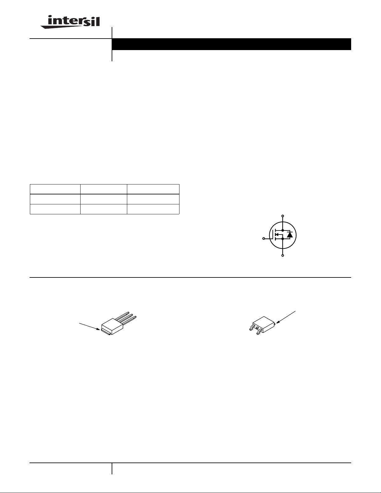
PART NUMBER PACKAGE BRAND
RFD4N06L TO-251AA RFD4N06L
RFD4N06LSM TO-252AA RFD4N06LSM
NOTE: When ordering, use the entire part number.
File Number
Features
• 4A, 60V
DS(ON)
= 0.600Ω
•r
• Design Optimized for 5 Volt Gate Drive
• Can be Driven Directly From Q-MOS, N-MOS,
or TTL Circuits
• SOA is Power Dissipation Limited
o
C Rated Junction Temperature
• 175
• Logic Level Gate
• High Input Impedance
• Related Literature
- TB334 “Guidelines for Soldering Surface Mount
Components to PC Boards”
Symbol
D
2837.1
Packaging
(FLANGE)
DRAIN
G
S
JEDEC TO-251AA JEDEC TO-252AA
SOURCE
DRAIN
GATE
GATE
SOURCE
DRAIN
(FLANGE)
6-189
CAUTION: These devices are sensitive to electrostatic discharge; follow proper ESD Handling Procedures.
http://www.intersil.com or 407-727-9207
| Copyright © Intersil Corporation 1999

RFD4N06L, RFD4N06LSM
Absolute Maximum Ratings T
= 25oC, Unless Otherwise Specified
C
RFD4N06L
RFD4N06LSM UNITS
Drain to Source Breakdown Voltage (Note 1) . . . . . . . . . . . . . . . . . . . . . . . . . . . . . . . . . . . . . . . . V
Drain to Gate Voltage (Note 1). . . . . . . . . . . . . . . . . . . . . . . . . . . . . . . . . . . . . . . . . . . . . . . . . . .V
Gate to Source Voltage . . . . . . . . . . . . . . . . . . . . . . . . . . . . . . . . . . . . . . . . . . . . . . . . . . . . . . . . . V
Continuous Drain Current . . . . . . . . . . . . . . . . . . . . . . . . . . . . . . . . . . . . . . . . . . . . . . . . . . . . . . . . .I
Pulsed Drain Current (Note 3) . . . . . . . . . . . . . . . . . . . . . . . . . . . . . . . . . . . . . . . . . . . . . . . . . . . . I
Maximum Power Dissipation . . . . . . . . . . . . . . . . . . . . . . . . . . . . . . . . . . . . . . . . . . . . . . . . . . . . . . P
DS
DGR
GS
D
DM
D
Derated above 25oC. . . . . . . . . . . . . . . . . . . . . . . . . . . . . . . . . . . . . . . . . . . . . . . . . . . . . . . . . . . . .
Operating and Storage Temperature . . . . . . . . . . . . . . . . . . . . . . . . . . . . . . . . . . . . . . . . . . . TJ,T
STG
Maximum Temperature for Soldering
Leads at 0.063in (1.6mm) from Case for 10s. . . . . . . . . . . . . . . . . . . . . . . . . . . . . . . . . . . . . . . . T
Package Body for 10s, See Techbrief 334 . . . . . . . . . . . . . . . . . . . . . . . . . . . . . . . . . . . . . . . . .T
CAUTION: Stresses above those listed in “Absolute Maximum Ratings” may cause permanent damage to the device. This is a stress only rating and operationofthe
device at these or any other conditions above those indicated in the operational sections of this specification is not implied.
L
pkg
60 V
60 V
±10V
4A
10 A
30
0.20
-55 to 175
300
260
W
W/oC
o
C
o
C
o
C
NOTE:
1. TJ= 25oC to 150oC.
Electrical Specifications T
= 25oC, Unless Otherwise Specified
C
PARAMETER SYMBOL TEST CONDITIONS MIN TYP MAX UNITS
Drain to Source Breakdown Voltage BV
Gate to Threshold Voltage V
Zero Gate Voltage Drain Current I
DSSID
GS(TH)VGS
DSS
= 1mA, VGS = 0V 60 - - V
= VDS, ID = 250µA 1 - 2.5 V
TC = 25oC, VDS = 50V, VGS = 0V - - 1 µA
TC = 125oC, VDS = 50V, VGS = 0V - - 50 µA
Gate to Source Leakage Current I
Drain to Source On Voltage (Note 2) V
GSS
DS(ON)ID
VGS = 10V, VDS = 0V - - 100 nA
= 1A, VGS = 5V - - 0.8 V
ID = 2A, VGS = 5V - - 2.0 V
ID = 4A, VGS = 7.5V - - 4.0 V
Drain to Source On Resistance (Note 2) r
Forward Transconductance (Note 2) V
Turn-On Delay Time t
DS(ON)ID
(plateau)
d(ON)VDD
Rise Time t
Turn-Off Delay Time t
d(OFF)
Fall Time t
Total Gate Charge
Q
g(TOT)VGS
(Gate to Source + Gate to Drain)
Gate Charge at 5V Q
Threshold Gate Charge Q
Thermal Resistance Junction to Case R
r
f
g(5)
g(TH)VGS
θJC
= 1A, VGS = 5V - - 0.600 Ω
VDS = 15V, ID = 4A - - 4.5 V
= 30V, ID = 1A, RGS = 6.25Ω,
VGS = 5V
- - 20 ns
- - 130 ns
- - 40 ns
- - 160 ns
= 0-10V VDD = 48V,
--8nC
ID = 2A,
VGS = 0-5V - - 5 nC
RL = 24Ω
= 0-1V - - 1 nC
--5oC/W
Source to Drain Diode Specifications
PARAMETER SYMBOL TEST CONDITIONS MIN TYP MAX UNITS
Source to Drain Diode Voltage (Note 2) V
Reverse Recovery Time t
NOTES:
2. Pulsed: pulse duration = 300µs max, duty cycle = 2%.
3. Repetitive rating: pulse width limited by maximum junction temperature.
6-190
ISD = 1A - - 1.4 V
SD
ISD = 2A, dISD/dt = 100A/µs - 150 - ns
rr
 Loading...