

Fairchild Semiconductor RFD16N06LESM Datasheet
RFD16N06LESM
Data Sheet September 2002
16A, 60V, 0.047 Ohm, Logic Level,
N-Channel Power MOSFETs
These are N-Channel power MOSFETs manu factured using
a modern process. This process, which uses feature sizes
approaching those of LSI integrated circuits gives optimum
utilization of silicon, resulting in outstanding performance.
They were designed for use in applications such as
switching regu la tors, switching converters, motor drivers,
relay drivers and emitter switches for bipolar transistors. This
performance is accomplished through a special gate oxide
design which provides full rated conductance at gate bias in
the 3V to 5V range, thereby facilitating true on-off power
control directly from logic level (5V) integrated circuits.
Formerly developmental type TA49027.
Ordering Information
PART NUMBER PACKAGE BRAND
RFD16N06LESM* TO-252AA 16N06LE
NOTE: When ordering, use the entire part number. Add suffix 9A to
obtain the TO-25 2AA v arian t in the t ape and re el, i.e . ,
RFD16N06LESM9A.
*RFD16N06LESM is only av a ilabe in tape and re el.
Features
• 16A, 60V
•r
• Temperature Compensating PSPICE
• Can be Driven Directly from CMOS, NMOS, TTL
Circuits
• Peak Current vs Pulse Width Curve
• UIS Rating Curve
• Related Literature
- TB334 “Guidelines for Soldering Surface Mount
= 0.047Ω
DS(ON)
Components to PC Boards”
®
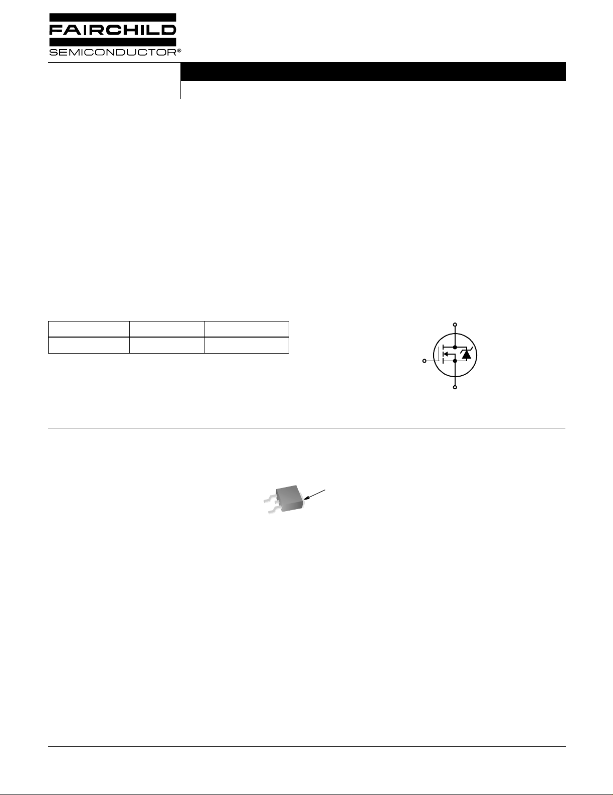
Model
Symbol
D
G
S
Packaging
JEDEC TO-252AA
DRAIN (FLANGE)
GATE
SOURCE
©2002 Fairchild Semiconductor Corporation RFD16N06LESM Rev. B1
RFD16N06LESM
Absolute Maximum Ratings T
= 25oC, Unless Otherwise Specified
C
RFD16N06LESM UNITS
Drain to Source Voltage (Note 1). . . . . . . . . . . . . . . . . . . . . . . . . . . . . . . . . . . . .V
Drain to Gate Voltage (R
= 20kΩ) (Note 1) . . . . . . . . . . . . . . . . . . . . . . . . . . V
GS
Gate to Source Voltage . . . . . . . . . . . . . . . . . . . . . . . . . . . . . . . . . . . . . . . . . . . . .V
Continuous Drain Current . . . . . . . . . . . . . . . . . . . . . . . . . . . . . . . . . . . . . . . . . . . . .I
Pulsed Drai n C u rr e n t (Note 3) . . . . . . . . . . . . . . . . . . . . . . . . . . . . . . . . . . . . . . I
Pulsed Avalanche Rating. . . . . . . . . . . . . . . . . . . . . . . . . . . . . . . . . . . . . . . . . . . .E
Power Dissipation . . . . . . . . . . . . . . . . . . . . . . . . . . . . . . . . . . . . . . . . . . . . . . . . . . P
Derate Above 25oC . . . . . . . . . . . . . . . . . . . . . . . . . . . . . . . . . . . . . . . . . . . . . . . . .
Operating and Storage Temperature . . . . . . . . . . . . . . . . . . . . . . . . . . . . . . . T
DSS
DGR
GS
D
DM
AS
D
, T
J
STG
Refer to Peak Current Curve
Maximum Tem perature for Soldering
Leads at 0.063in (1.6mm) from Case for 10s. . . . . . . . . . . . . . . . . . . . . . . . . . . . T
Package Body for 10s, See Techbrief 334 . . . . . . . . . . . . . . . . . . . . . . . . . . . . .T
CAUTION: Stresses above those listed in “A bsolute Maximu m Rating s” may cause per manent d amage to t he device. This is a str ess on ly rating and operation o f the
device at these or any other conditions above those indicated in the operational sections of this specification is not implied.
L
pkg
60 V
60 V
+10, -8 V
16
Refer to UIS Cu r ve
90
0.606
-55 to 175
300
260
A
W
W/oC
o
C
o
C
o
C
NOTE:
= 25oC to 150oC.
1. T
J
Electrical Specifications T
= 25oC, Unless Otherwise Specified
C
PARAMETER SYMBOL TEST CONDITIONS MIN TYP MAX UNITS
Drain to Source Breakdown Voltage BV
Gate Threshold Voltage V
GS(TH)
Zero Gate Voltage Drain Current I
Gate to Source Leakage Current I
Drain to Source On Resistance (Note 2) r
DS(ON)ID
Turn-On Time t
Turn-On Delay Time t
d(ON)
Rise Time t
Turn-Off Delay Time t
d(OFF)
Fall Time t
Turn-Off Time t
Total Gate Charge Q
g(TOT)
Gate Charge at 5V Q
Threshold Gate Charge Q
Input Capacitance C
Output Capacitance C
Reverse Transfer Capacitance C
Thermal Resistance Junction to Case R
Thermal Resistance Junction to Ambient R
DSS
DSS
GSS
ON
r
f
OFF
g(5)
g(TH)
ISS
OSS
RSS
θJC
θJA
ID = 250µA, VGS = 0V, Figure 11 60 - - V
VGS = VDS, ID = 250µA, Figure 10 1 - 3 V
VDS = 55V, VGS = 0V - - 1 µA
V
= 50V, VGS = 0V, TC = 150oC - - 250 µA
DS
VGS = +10, -8V - - 10 µA
= 16A, VGS = 5V - - 0.047 Ω
VDD = 30V, ID = 16A, RL = 1.88Ω,
V
= 5V, RGS = 5Ω
GS
Figures 16, 17
- - 100 ns
-11- ns
-60- ns
-48- ns
-35- ns
- - 115 ns
VGS = 0V to 10V VDD = 48V,
I
= 16A, RL = 3Ω
VGS = 0V to 5V - 29 35 nC
D
Figures 18, 19
-5162nC
VGS = 0V to 1V - 1.8 2.6 nC
VDS = 25V, VGS = 0V,
f = 1MHz
Figure 12
- 1350 - pF
- 300 - pF
-90- pF
- - 1.65
TO-251AA, TO-252AA - - 80
o
o
C/W
C/W
Source to Drain Diode Specifications
PARAMETER SYMBOL TEST CONDITIONS MIN TYP MAX UNITS
Source to Drain Diode Voltage (Note 2) V
Diode Reverse Recovery Time t
SD
rr
NOTES:
2. Pulse Test: Pulse Width ≤ 300µs , Duty Cycle ≤ 2%.
3. Repetitive Rating: Pulse Width limited by max junction temperature.
©2002 Fairchild Semiconductor Corporation RFD16N06LESM Rev. B1
ISD = 16A - - 1.5 V
ISD = 16A, dISD/dt = 100A/µs - - 125 ns
RFD16N06LESM
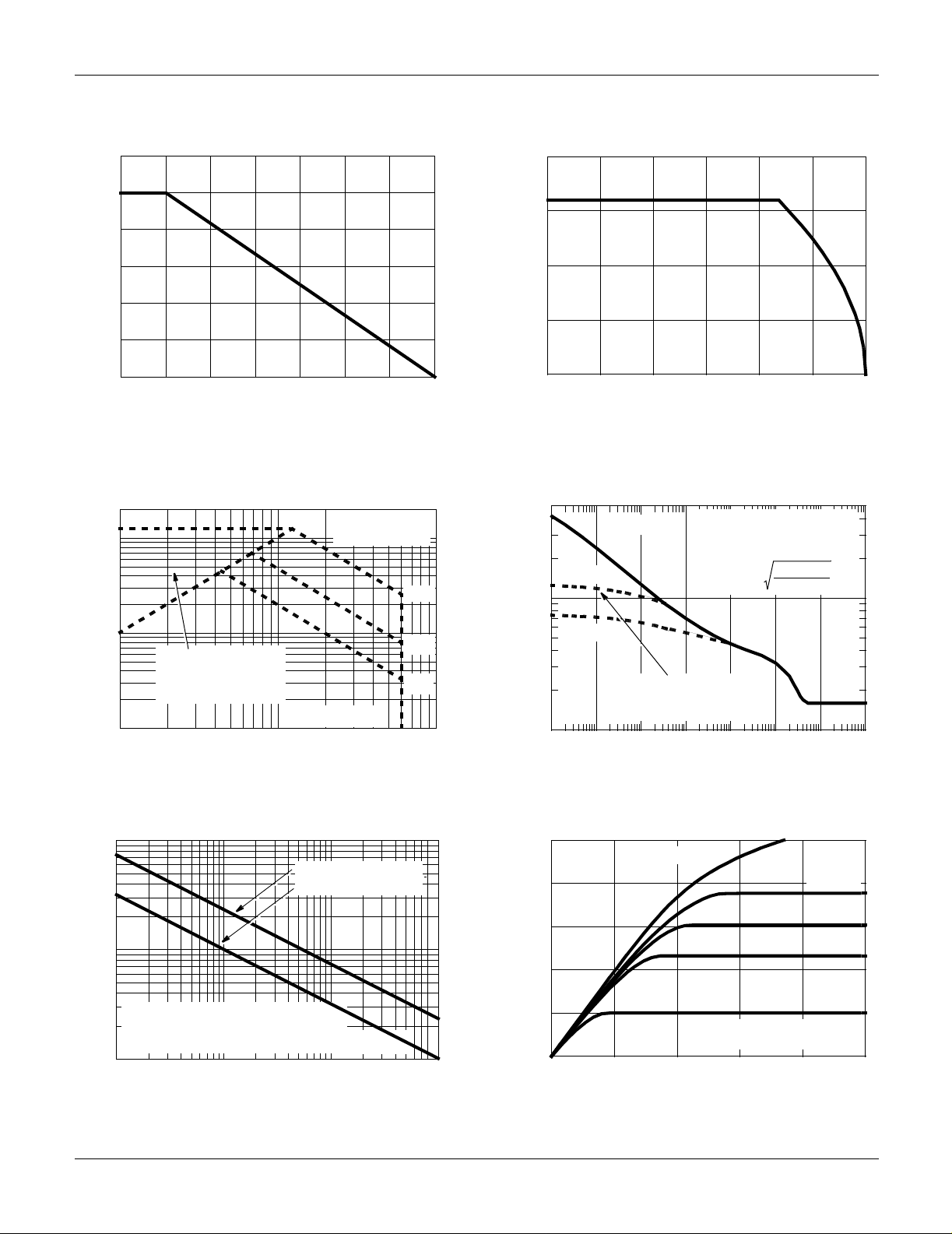
Typical Performance Curves Unless Otherwise Specified
1.2
1.0
0.8
0.6
0.4
0.2
POWER DISSIPATION MULTIPLIER
0
25 50 75 100
0
TC, CASE TEMPERATURE (oC)
125
150
FIGURE 1. NORMALIZED PO WER DISSIP ATION vs CASE
TEMPERATURE
200
100
TC = 25oC
T
= MAX RATED
J
100µs
20
15
10
, DRAIN CURRENT (A)
D
5
I
0
1750
25
50
75 100 125 150 175
TC, CASE TEMPERATURE (oC)
FIGURE 2. MAXIMUM CONTINUOUS DRAIN CURRENT vs
CASE TEMPERATURE
500
TC = 25oC
VGS = 10V
100
FOR TEMPERATURES
ABOVE 25
CURRENT AS FOLLOWS:
I = I
o
25
(
C DERATE PEAK
175 - T
C
150
)
10
DRAIN CURRENT (A)
D,
I
1
OPERATION IN THIS
AREA MAY BE
LIMITED BY r
110
VDS, DRAIN TO SOURCE VOLTAGE (V)
DS(ON)
V
DSS
MAX = 60V
1ms
10ms
100
VGS = 5V
, PEAK CURRENT CAPABILITY (A)
DM
I
10
-6
10
TRANSCONDUCTANCE
MAY LIMIT CURRENT
IN THIS REGION
-4
-5
10
10
t, PULSE WIDTH (s)
-2
-3
10
10
FIGURE 3. FORWARD BIAS SAFE OPERATING AREA FIGURE 4. PEAK CURRENT CAPABILITY
100
STAR TING T
STARTING TJ = 150oC
10
AVALANCHE CURRENT (A)
If R = 0
,
tAV = (L)(IAS)/(1.3*RATED BV
AS
I
If R ≠ 0
t
= (L/R)ln[(IAS*R)/(1.3*RATED BV
AV
1
0.01 0.1 1 10
tAV, TIME IN AVALANCHE (ms)
DSS
- VDD)
DSS
= 25oC
J
- VDD) +1]
100
T
=25oC
C
80
60
40
, DRAIN CURRENT (A)
D
I
20
0
0 1.5 3.0 4.5 6.0 7.5
VDS, DRAIN TO SOURCE VOLTAGE (V)
VGS = 10V
PULSE DURATION = 80µs
DUTY CYCLE = 0.5% MAX.
10-110
VGS = 5V
V
V
V
0
GS
GS
GS
= 4.5V
= 4V
= 3V
1
10
FIGURE 5. UNCLAMPED INDUCTIVE SWITCHING FIGURE 6. SATURATION CHARACTERISTICS
©2002 Fairchild Semiconductor Corporation RFD16N06LESM Rev. B1
 Loading...