

Fairchild Semiconductor RFD16N05LSM Datasheet
GATE
SOURCE
DRAIN (FLANGE)
RFD16N05L, RFD16N05LSM
Data Sheet January 2002
16A, 50V, 0.047 Ohm, Logic Level,
N-Channel Power MOSFETs
These are N-Channel logic level power MOSFETs
manufactured using the MegaFET process. This process,
which uses feature sizes approaching those of LSI
integrated circuits gives optimum utilization of silicon,
resulting in outstanding performance. They were designed
for use with logic level (5V) driving sources in applications
such as programmable controllers, automotive switching,
switching regulators, switching converters, motor relay
drivers and emitter switches for bipolar transistors. This
performance is accomplished through a special gate oxide
design which provides full rated conductance at gate biases
in the 3V to 5V range, thereby facilitating true on-off power
control directly from logic circuit supply voltages.
Formerly developmental type TA09871.
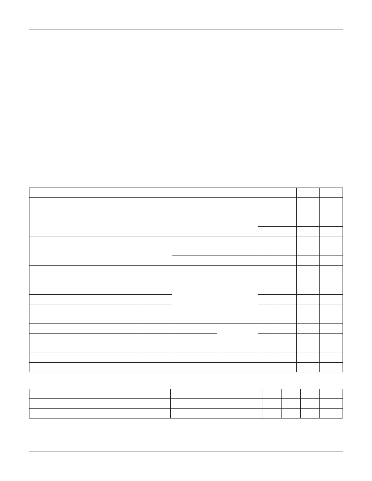
Ordering Information
PART NUMBER PACKAGE BRAND
RFD16N05L TO-251AA RFD16N05L
RFD16N05LSM TO-252AA RFD16N05LSM
NOTE: When ordering, include the entire part number. Add the suffix 9A
to obtain the TO-252AA variant in tape and reel, i.e. RFD16N05LSM9A
Features
• 16A, 50V
•r
• UIS SOA Rating Curve (Single Pulse)
• Design Optimized for 5V Gate Drives
• Can be Driven Directly from CMOS, NMOS, TTL Circuits
• Compatible with Automotive Drive Requirements
• SOA is Power Dissipation Limited
• Nanosecond Switching Speeds
• Linear Transfer Characteristics
• High Input Impedance
• Majority Carrier Device
• Related Literature
- TB334 “Guidelines for Soldering Surface Mount
= 0.047 Ω
DS(ON)
Components to PC Boards”
Symbol
D
Packaging
DRAIN (FLANGE)
G
S
JEDEC TO-251AA JEDEC TO-252AA
SOURCE
DRAIN
GATE
©2002 Fairchild Semiconductor Corporation RFD16N05L, RFD16N05LSM Rev. B
±
= ±
Ω
Ω
θ
θ
RFD16N05L, RFD16N05LSM
Absolute Maximum Ratings
o
T
= 25
C, Unless Otherwise Specified
C
RFD16N05L,
RFD16N05LSM UNITS
Drain to Source Voltage (Note 1) . . . . . . . . . . . . . . . . . . . . . . . . . . . . . . . . . . . . . . . . . . . V
Drain to Gate Voltage (R
= 20k Ω ) (Note 1) . . . . . . . . . . . . . . . . . . . . . . . . . . . . . . . . V
GS
Continuous Drain Current . . . . . . . . . . . . . . . . . . . . . . . . . . . . . . . . . . . . . . . . . . . . . . . . . . I
Pulsed Drain Current (Note 3) . . . . . . . . . . . . . . . . . . . . . . . . . . . . . . . . . . . . . . . . . . . .I
Gate to Source Voltage . . . . . . . . . . . . . . . . . . . . . . . . . . . . . . . . . . . . . . . . . . . . . . . . . . V
Maximum Power Dissipation . . . . . . . . . . . . . . . . . . . . . . . . . . . . . . . . . . . . . . . . . . . . . . . P
Derate Above 25
o
C . . . . . . . . . . . . . . . . . . . . . . . . . . . . . . . . . . . . . . . . . . . . . . . . . . . . . . . .
Operating and Storage Temperature . . . . . . . . . . . . . . . . . . . . . . . . . . . . . . . . . . . . T
DS
DGR
D
DM
GS
D
, T
J
STG
Maximum Temperature for Soldering
Leads at 0.063in (1.6mm) from Case for 10s. . . . . . . . . . . . . . . . . . . . . . . . . . . . . . . . . . T
Package Body for 10s, See Techbrief 334 . . . . . . . . . . . . . . . . . . . . . . . . . . . . . . . . . . T
CAUTION: Stresses above those listed in “Absolute Maximum Ratings” may cause permanent damage to the device. This is a stress only rating and operation of the
device at these or any other conditions above those indicated in the operational sections of this specification is not implied.
L
pkg
50 V
50 V
16
45
10 V
60
0.48
-55 to 150
300
260
W/
A
A
W
o
C
o
C
o
C
o
C
NOTE:
J
= 25
o
C to 125
1. T
Electrical Specifications
o
C.
o
T
= 25
C, Unless Otherwise Specified
C
PARAMETER SYMBOL TEST CONDITIONS MIN TYP MAX UNITS
Drain to Source Breakdown Voltage BV
Gate to Threshold Voltage V
GS(TH)
Zero Gate Voltage Drain Current I
Gate to Source Leakage Current I
Drain to Source On Resistance (Note 2) r
DS(ON)
Turn-On Time t
Turn-On Delay Time t
d(ON)
Rise Time t
Turn-Off Delay Time t
d(OFF)
Fall Time t
Turn-Off Time t
Total Gate Charge Q
(OFF)
g(TOT)
Gate Charge at 5V Q
Threshold Gate Charge Q
Thermal Resistance Junction to Case R
Thermal Resistance Junction to Ambient R
DSS
DSS
GSS
(ON)
g(5)
g(TH)
I
r
= 250mA, V
D
V
= V
GS
DS
V
= 40V, V
DS
T
= 150
C
V
10V, V
GS
I
= 16A, V
D
I
= 16A, V
D
V
= 25V, I
DD
V
5V, R
GS =
Figures 15, 16
= 0V, Figure 10 50 - - V
GS
, I
= 250mA, Figure 9 1 - 2 V
D
= 0V
GS
o
C
= 0V - - 100 nA
DS
= 5V - - 0.047
GS
= 4V - - 0.056
GS
= 8A,
D
= 12.5 Ω
GS
-- 1 µ A
--50 µ A
- - 60 ns
-14 - ns
-30 - ns
-42 - ns
f
-14 - ns
- - 100 ns
V
= 0V to 10V V
GS
V
= 0V to 5V - - 45 nC
GS
V
= 0V to 1V - - 3 nC
GS
JC
- - 100
JA
= 40V,
DD
I
= 16A,
D
R
= 2.5 Ω
L
Figures 17, 18
- - 80 nC
- - 2.083
o
o
C/W
C/W
Source to Drain Diode Specifications
PARAMETER SYMBOL TEST CONDITIONS MIN TYP MAX UNITS
Source to Drain Diode Voltage V
Diode Reverse Recovery Time t
SD
rr
NOTES:
2. Pulse Test: Pulse Width ≤ 300ms, Duty Cycle ≤ 2%.
3. Repetitive Rating: Pulse Width limited by max junction temperature.
©2002 Fairchild Semiconductor Corporation RFD16N05L, RFD16N05LSM Rev. B
I
= 16A - - 1.5 V
SD
I
= 16A, dI
SD
/dt = 100A/ µ s - - 125 ns
SD
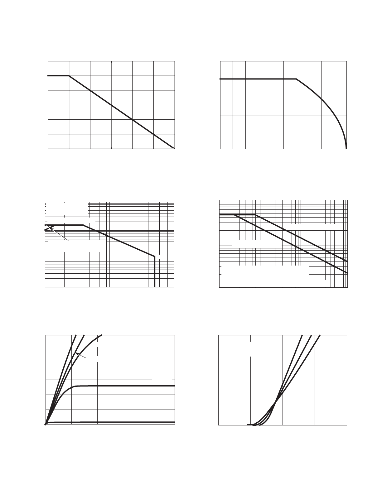
TC, CASE TEMPERATURE (oC)
I
D
, DRAIN CURRENT (A)
0
25 50 75 100 150
5
10
20
125
15
10
10
2
1
I
AS
, AVALANCHE CURRENT (A)
tAV, TIME IN AVALANCHE (ms)
1100.01 0.10
tAV = (L)(IAS)/(1.3 RATED BV
DSS
- VDD)
If R = 0
If R ≠ 0
t
AV
= (L/R)ln[(IAS*R)/(1.3 RATED BV
DSS
- VDD) +1]
STARTING TJ = 25oC
STARTING TJ = 150oC
Idm
0 3.0 4.5 6.01.5
0
15
30
45
I
DS(ON)
, DRAIN TO SOURCE ON CURRENT (A)
VGS, GATE TO SOURCE VOLTAGE (V)
PULSE DURATION = 80µs
DUTY CYCLE = 0.5% MAX
V
DS
= 15V
RFD16N05L, RFD16N05LSM
Typical Performance Curves
1.2
1.0
0.8
0.6
0.4
0.2
POWER DISSIPATION MULTIPLIER
0
0 25 50 75 100 150
TC, CASE TEMPERATURE (oC)
Unless Otherwise Specified
125
FIGURE 1. NORMALIZED POWER DISSIPATION vs CASE
TEMPERATURE
2
10
TC = 25oC
TJ = MAX RATED
ID MAX CONTINUOUS
10
FIGURE 2. MAXIMUM CONTINUOUS DRAIN CURRENT vs
CASE TEMPERATURE
1
, DRAIN CURRENT (A)
D
I
0.1
1
FIGURE 3. FORWARD BIAS SAFE OPERATING AREA FIGURE 4. UNCLAMPED INDUCTIVE SWITCHING SOA
45
30
15
, DRAIN TO SOURCE CURRENT (A)
DS
I
0
0 1.5 3.0 4.5 7.5
OPERATION IN THIS AREA
LIMITED BY r
VGS = 10V
DS(ON)
VDS, DRAIN TO SOURCE VOLTAGE (V)
VGS = 4V
VGS = 5V
VDS, DRAIN TO SOURCE VOLTAGE (V)
10
PULSE DURATION = 80µs
DUTY CYCLE = 0.5% MAX.
6.0
DC
TC = 25oC
VGS = 3V
VGS = 2V
2
10
(SINGLE PULSE UIS SOA)
©2002 Fairchild Semiconductor Corporation RFD16N05L, RFD16N05LSM Rev. B
FIGURE 5. SATURATION CHARACTERISTICS FIGURE 6. TRANSFER CHARACTERISTICS
 Loading...