

Fairchild Semiconductor RF1S640SM Datasheet
IRF640, RF1S640, RF1S640SM
Data Sheet January 2002
18A, 200V, 0.180 Ohm, N-Channel Power
MOSFETs
These are N-Channel enhancement mode silicon gate
power field effect transistors. They are advanced power
MOSFETs designed, tested, and guaranteed to withstand a
specified level of energy in the breakdown avalanche mode
of operation. All of these power MOSFETs are designed for
applications such as switchi ng r egu lators, switching
convertors, motor drivers, relay drivers, and drivers for high
power bipolar switching transistors requiring high speed and
low gate drive power. These types can be operated directly
from integrated circuits.
Formerly developmental type TA17422.
Ordering Information
PART NUMBER PACKAGE BRAND
IRF640 TO-220AB IRF640
RF1S640 TO-262AA RF1S640
RF1S640SM TO-263AB RF1S640
NOTE: When ordering, use the ent ire part number . Add t he suffix 9A t o
obtain the TO-263AB variant in the tape and reel, i.e., RF1S6 4 0SM9A.
Features
• 18A, 200V
•r
DS(ON)
= 0.180Ω
• Single Pulse Avalanche Energy Rated
• SOA is Power Dissipation Limited
• Nanosecond Switc hi ng Spee d
• Linear Transfer Characteristics
• High Input Impedance
• Related Literature
- TB334 “Guidelines for Soldering Surface Moun t
Components to PC Boards”
Symbol
D
G
S
Packaging
DRAIN (FLANGE)
JEDEC TO-220AB JEDEC TO-263AB
SOURCE
DRAIN
GATE
JEDEC TO-262AA
DRAIN
(FLANGE)
SOURCE
DRAIN
GATE
GATE
SOURCE
DRAIN
(FLANGE)
©2001 Fairchild Semiconductor Corpo ration IRF640, RF1S640, RF1S640SM Rev. B
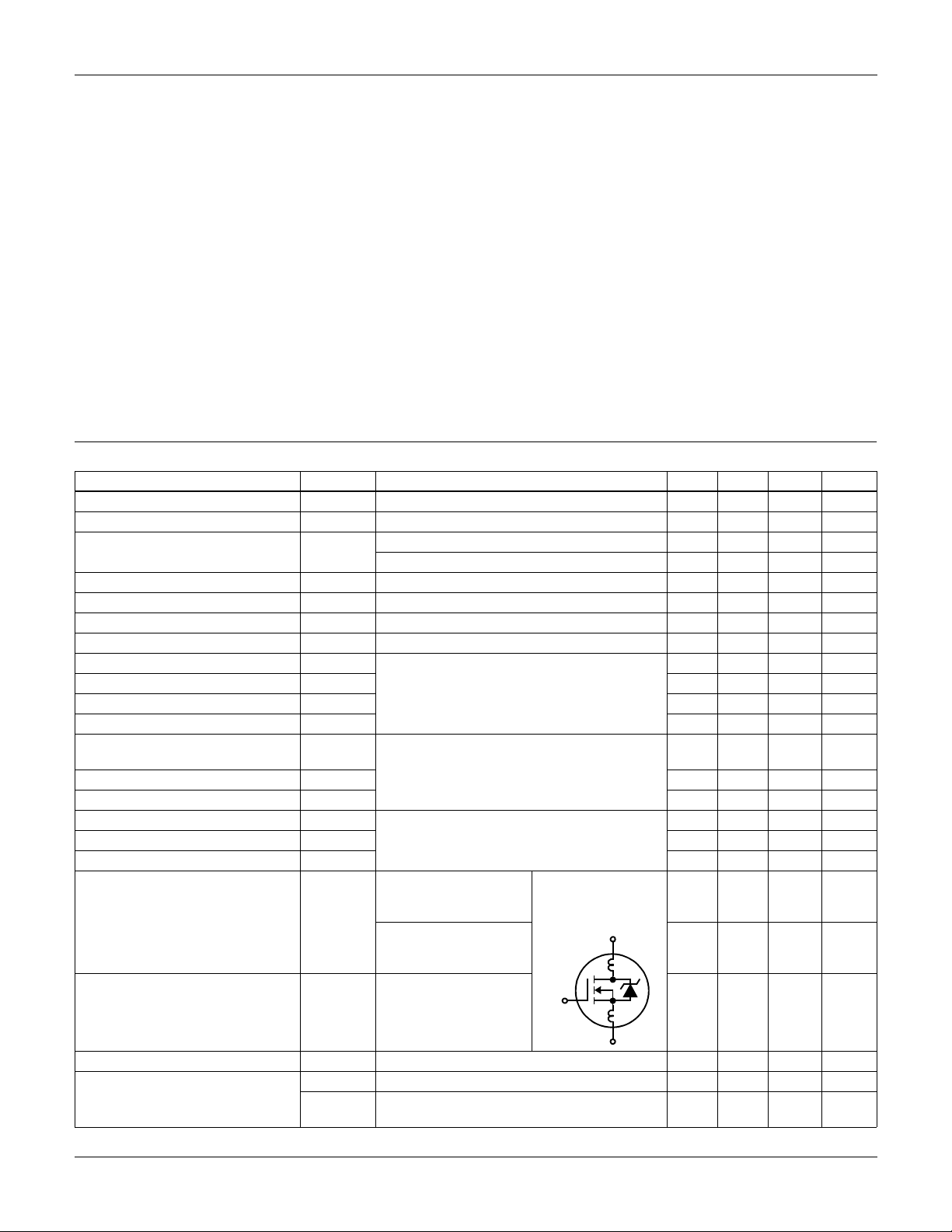
G
D
IRF640, RF1S640, RF1S640SM
Absolute Maximum Ratings
TC = 25oC, Unless Otherwise Specified
IRF640, RF1S640, RF1S640SM UNITS
Drain to Source Breakdown Voltage (Note 1) . . . . . . . . . . . . . . . . . . . . . . . . . . . . . . . . . V
Drain to Gate Voltage (R
= 20kΩ) (Note 1) . . . . . . . . . . . . . . . . . . . . . . . . . . . . . . . V
GS
Continuous Drain Current . . . . . . . . . . . . . . . . . . . . . . . . . . . . . . . . . . . . . . . . . . . . . . . . . I
TC = 100oC . . . . . . . . . . . . . . . . . . . . . . . . . . . . . . . . . . . . . . . . . . . . . . . . . . . . . . . . . . I
Pulsed Drain Current (Note 3) . . . . . . . . . . . . . . . . . . . . . . . . . . . . . . . . . . . . . . . . . . . . . I
Gate to Source Voltage . . . . . . . . . . . . . . . . . . . . . . . . . . . . . . . . . . . . . . . . . . . . . . . . . . V
Maximum Power Dissipation . . . . . . . . . . . . . . . . . . . . . . . . . . . . . . . . . . . . . . . . . . . . . . . P
DS
DGR
D
D
DM
GS
D
Dissipation Derating Factor . . . . . . . . . . . . . . . . . . . . . . . . . . . . . . . . . . . . . . . . . . . . . . . . 1.0 W/
Single Pulse Avalanche Energy Rating (Note 4). . . . . . . . . . . . . . . . . . . . . . . . . . . . . . . . . E
Operating and Storage Temperature . . . . . . . . . . . . . . . . . . . . . . . . . . . . . . . . . . . . T
AS
, T
J
STG
Maximum Temperature for Soldering
Leads at 0.063in (1.6mm) from Case for 10s. . . . . . . . . . . . . . . . . . . . . . . . . . . . . . . . . T
Package Body for 10s, See TB334. . . . . . . . . . . . . . . . . . . . . . . . . . . . . . . . . . . . . . . T
CAUTION: Stresses above those listed in “A bsolute Maximu m Rating s” may cause per manen t damage to the device. This is a stress on ly rating and operat ion of the
device at these or any other conditions above those indica ted in the operational sections of this specification is not implied.
L
pkg
200 V
200 V
18
11
72 A
±20 V
125 W
580 mJ
-55 to 150
300
260
A
A
o
C
o
C
o
C
o
C
NOTE:
1. T
= 25oC to 125oC.
J
Electrical Specifications
TC = 25oC, Unless Otherwise Specified
PARAMETER SYMBOL TEST CONDITIONS MIN TYP MAX UNITS
Drain to Source Breakdown Voltage BV
Gate Threshold Voltage V
GS(TH)VGS
Zero Gate Voltage Drain Current I
On-State Drain Current (Note 1) I
D(ON)
Gate to Source Leakage Current I
Drain to Source On Resistance (Note 1) r
DS(ON)ID
Forward Transconductance (Note 1) g
Turn-On Delay Time t
d(ON)
Rise Time t
Turn-Off Delay Time t
d(OFF)
Fall Time t
Total Gate Charge
(Gate to Source + Gate to Drain)
Q
g(TOT)VGS
Gate to Source Charge Q
Gate to Drain “Miller” Charge Q
Input Capacitance C
Output Capacitance C
Reverse Transfer Capacitance C
Internal Drain Inductance L
DSSID
DSS
GSS
fs
r
f
gs
gd
ISS
OSS
RSS
D
= 250µA, VGS = 0V, (Figure 10) 200 - - V
= VDS, ID = 250µA2-4V
VDS = Rated BV
= 0.8 x Rated BV
V
DS
VDS > I
D(ON)
, VGS = 0V - - 25 µA
DSS
, VGS = 0V, TJ = 125oC - - 250 µA
DSS
x r
DS(ON)MAX
, VGS = 10V (Figure 7) 18 - - A
VGS = ±20V - - ±100 nA
= 10A, VGS = 10V (Figures 8, 9) - 0.14 0.18 Ω
VDS ≥ 10V, ID = 11A (Figure 12) 6.7 10 - S
VDD = 100V, ID ≈ 18A, RGS = 9.1Ω, RL = 5.4Ω,
MOSFET Switching Times are Essentially
Independent of Operating Temperature
-1321ns
-5077ns
-4668ns
-3554ns
= 10V, ID ≈ 18A, VDS = 0.8 x Rated BV
(Figure 14) Gate Charge is Essentially Independent
DSS
of Operating Temperature
I
= 1.5mA
G(REF)
-4364nC
-8-nC
-22- nC
VDS = 25V, VGS = 0V, f = 1MHz (Figure 11) - 1275 - pF
- 400 - pF
- 100 - pF
Measured From the
Contact Screw on Tab to
Center of Die
Measured From the Drain
Modified MOSFET
Symbol Showing the
Internal Devices
Inductances
-3.5- nH
-4.5- nH
Lead, 6mm (0.25in) From
Internal Source Inductance L
Package to Center of Die
Measured From the
S
L
D
-7.5- nH
Source Lead, 6mm
L
S
S
--1oC/W
o
C/W
--62oC/W
Thermal Resistance Junction to Case R
Thermal Resistance Junction to
Ambient
(0.25in) from Header to
Source Bonding Pad
θJC
R
θJA
R
θJA
Free Air Operation, IRF640 - - 62
RF1S640SM Mounted on FR-4 Board with Minimum
Mounting Pad
©2001 Fairchild Semiconductor Corpo ration IRF640, RF1S640, RF1S640SM Rev. B
Source to Drain Diode Specifications
D
S
0
POWER DISSIPATION MULTIPLIER
0
PARAMETER SYMBOL TEST CONDITIONS MIN TYP MAX UNITS
Continuous Source to Drain Current I
Pulse Source to Drain Current
(Note 2)
I
IRF640, RF1S640, RF1S640SM
SD
SDM
Modified MOSFET
Symbol Showing the
Integral Reverse P-N
Junction Diode
G
--18A
--72A
Source to Drain Diode Voltage (Note 2) V
Reverse Recovery Time t
Reverse Recovery Charge Q
SD
RR
TJ = 25oC, ISD = 18A, VGS = 0V, (Figure 13) - - 2. 0 V
TJ = 25oC, ISD = 18A, dISD/dt = 100A/µs 120 240 530 ns
rr
TJ = 25oC, ISD = 18A, dISD/dt = 100A/µs1.32.85.6µC
NOTES:
2. Pulse Test: Pulse width ≤ 300µs, duty cycle ≤ 2%.
3. Repetitive Ra ting: Pulse width limited b y maximum junction temperature. See Transient Thermal Impedance curve (Figure 3).
= 50V, starting TJ = 25oC, L = 3.37mH, RG = 25Ω, peak IAS = 18A.
4. V
DD
Typical Performance Curves
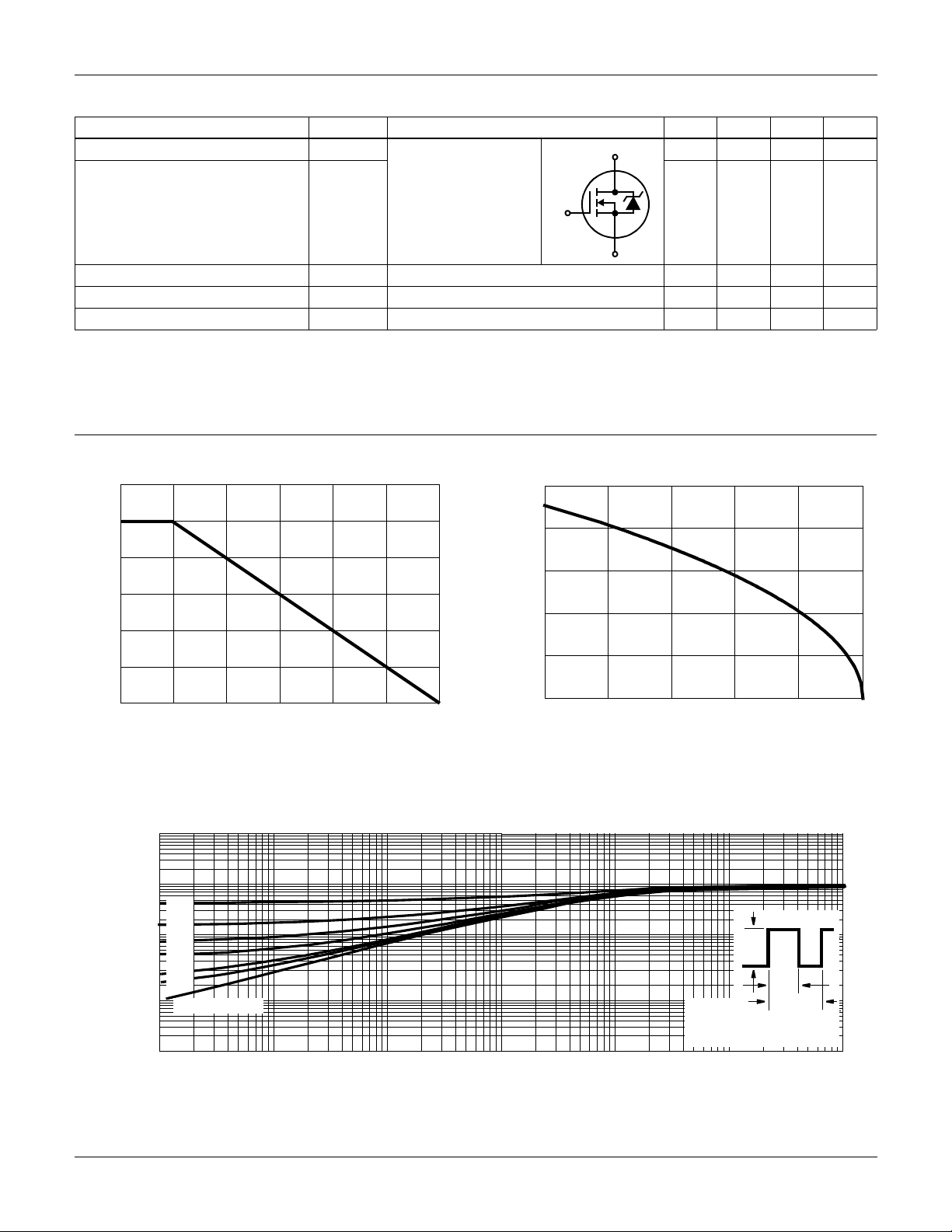
1.2
1.0
0.8
0.6
0.4
0.2
0
0 50 100 15
T
, CASE TEMPERATURE (oC)
C
Unless Otherwise Specified
20
16
12
8
, DRAIN CURRENT (A)
D
I
4
0
25 50 75 100
TC, CASE TEMPERATURE (oC)
125
15
FIGURE 1. NORMALIZED POWER DISSIPATION vs CASE
TEMPERATURE
10
1
C/W)
o
, TRANSIENT
θJC
Z
THERMAL IMPEDANCE (
©2001 Fairchild Semiconductor Corpo ration IRF640, RF1S640, RF1S640SM Rev. B
0 . 1
0.01
0.001
0.5
0.2
0.1
0.05
0.02
0.01
SINGLE PULSE
-5
-4
10
-3
10
tP, RECTANGULAR PULSE DURATION (s)
FIGURE 3. MAXIMUM TRANSIENT THERMAL IMPEDANCE
FIGURE 2. MAXIMUM CONTINUOUS DRAIN CURRENT vs
CASE TEMPERATURE
P
DM
t
1
t
NOTES:
DUTY FACTOR: D = t
PEAK TJ = PDM x Z
-2
10
-1
10
110
2
θJC
1/t2
+ T
C
10
 Loading...