

Fairchild Semiconductor RF1S45N06 Datasheet
RFG45N06, RFP45N06,
SEMICONDUCTOR
RF1S45N06, RF1S45N06SM
December 1995
Features
• 45A, 60V
•r
•
= 0.028Ω
DS(ON)
Temperature Compensating
PSPICE Model
• Peak Current vs Pulse Width Curve
• UIS Rating Curve
o
• +175
C Operating Temperature
Description
The RFG45N06, RFP45N06, RF1S45N06, RF1S45N06SM
N-Channel power MOSFETs are manufactured using the
MegaFET process. This process, which uses feature sizes
approaching those of LSI integrated circuits gives optimum
utilization of silicon, resulting in outstanding performance.
They were designed for use in applications such as switching regulators, switching converters, motor drivers, relay
drivers and emitter switches for bipolar transistors. These
transistors can be operated directly from integrated circuits.
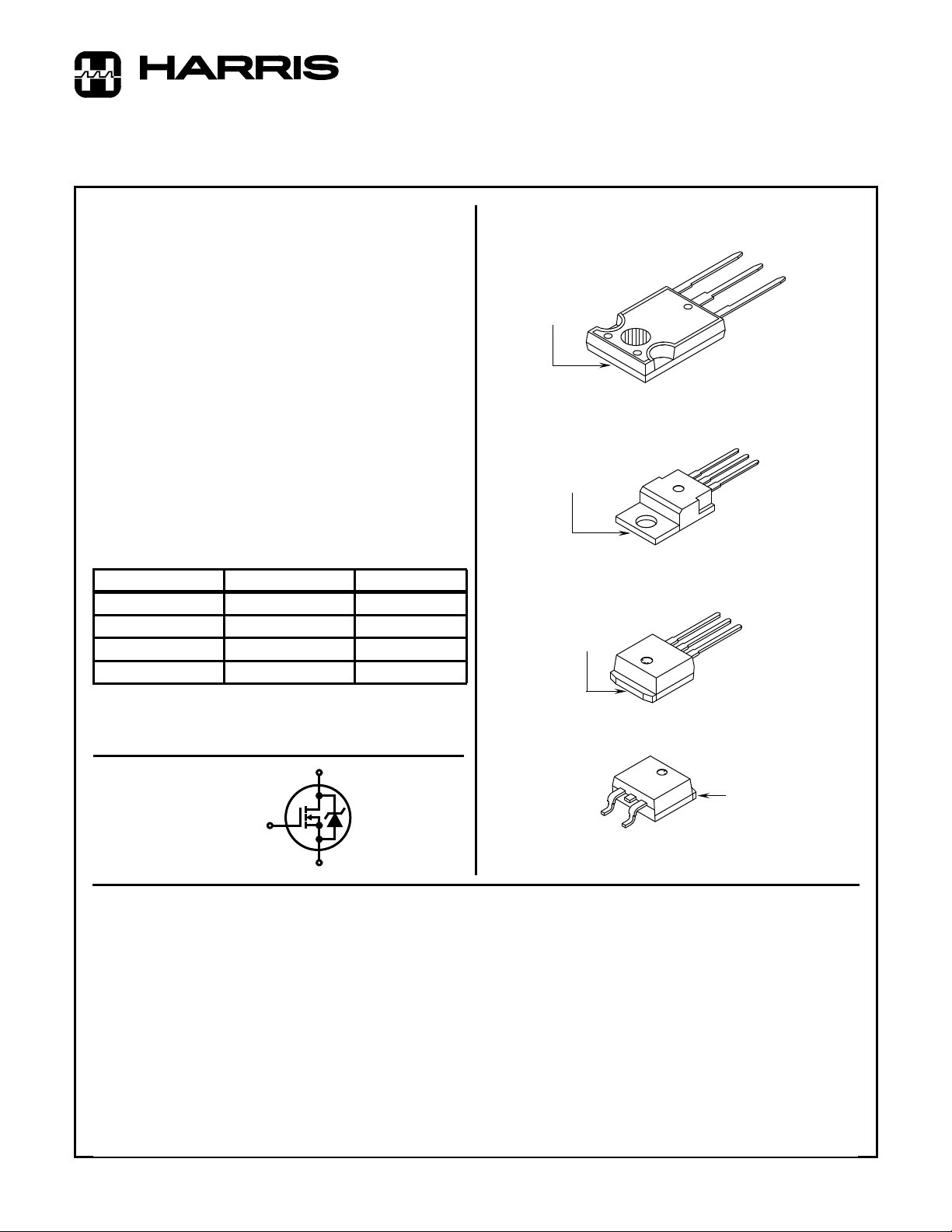
PACKAGE AVAILABILITY
PART NUMBER PACKAGE BRAND
RFG45N06
RFP45N06
RF1S45N06
RF1S45N06SM
NOTE: When ordering, use the entire part number. Add the suf fix, 9A,
to obtain the TO-263AB variant in tape and reel, i.e.RF1S45N06SM9A.
Formerly developmental type TA49028.
Symbol
TO-247 RFG45N06
TO-220AB RFP45N06
TO-262AA F1S45N06
TO-263AB F1S45N06
D
G
45A, 60V, Avalanche Rated N-Channel
Enhancement-Mode Power MOSFETs
Packages
JEDEC STYLE TO-247
SOURCE
DRAIN
DRAIN
GATE
GATE
GATE
DRAIN
(BOTTOM
SIDE METAL)
DRAIN
(FLANGE)
DRAIN
(FLANGE)
GATE
SOURCE
JEDEC TO-220AB
JEDEC TO-262AA
A
JEDEC TO-263AB
A
M
A
SOURCE
SOURCE
DRAIN
DRAIN
(FLANGE)
S
Absolute Maximum Ratings T
Drain Source Voltage . . . . . . . . . . . . . . . . . . . . . . . . . . . . . . . . . . . . . . . . . . . . . V
Drain Gate Voltage. . . . . . . . . . . . . . . . . . . . . . . . . . . . . . . . . . . . . . . . . . . . . . .V
Gate Source Voltage . . . . . . . . . . . . . . . . . . . . . . . . . . . . . . . . . . . . . . . . . . . . . . V
Drain Current
RMS Continuous. . . . . . . . . . . . . . . . . . . . . . . . . . . . . . . . . . . . . . . . . . . . . . . . . .I
Pulsed Drain Current . . . . . . . . . . . . . . . . . . . . . . . . . . . . . . . . . . . . . . . . . . . . .I
Pulsed Avalanche Rating . . . . . . . . . . . . . . . . . . . . . . . . . . . . . . . . . . . . . . . . . . . E
Maximum Avalanche Current. . . . . . . . . . . . . . . . . . . . . . . . . . . . . . . . . . . . . . . . .I
Power Dissipation
= +25oC. . . . . . . . . . . . . . . . . . . . . . . . . . . . . . . . . . . . . . . . . . . . . . . . . . . . . P
T
C
Derate above +25oC. . . . . . . . . . . . . . . . . . . . . . . . . . . . . . . . . . . . . . . . . . . . . . P
Operating and Storage Temperature . . . . . . . . . . . . . . . . . . . . . . . . . . . . . . T
CAUTION: These devices are sensitive to electrostatic discharge. Users should follow proper ESD handling procedures.
Copyright
© Harris Corporation 1995
= +25oC
C
3-33
STG
DSS
DGR
GS
DM
AS
AM
, T
RFG45N06, RFP45N06
RF1S45N06, RF1S45N06SM UNITS
D
Refer to Peak Current Curve
Refer to UIS Curve
D
T
J
60 V
60 V
±20 V
45
125 A
131
0.877
-55 to +175
File Number 3574.2
A
W
W/oC
o
C
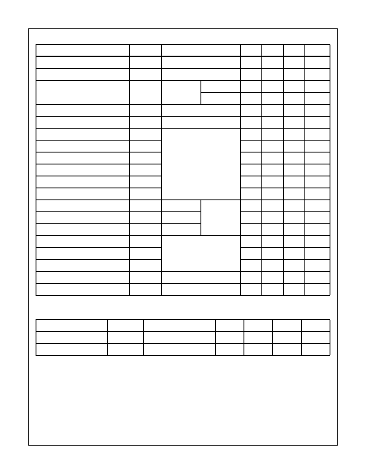
Specifications RFG45N06, RFP45N06, RF1S45N06, RF1S45N06SM
Electrical Specifications T
= +25oC, Unless Otherwise Specified
C
PARAMETER SYMBOL TEST CONDITIONS MIN TYP MAX UNITS
Drain-Source Breakdown Voltage BV
Gate Threshold Voltage V
Zero Gate Voltage Drain Current I
Gate-Source Leakage Current I
On Resistance r
Turn-On Time t
Turn-On Delay Time t
Rise Time t
Turn-Off Delay Time t
Fall Time t
Turn-Off Time t
Total Gate Charge Q
Gate Charge at 10V Q
DSS
GS(TH)
DSS
GSS
DS(ON)
ON
D(ON)
R
D(OFF)
F
OFF
G(TOT)
G(10)
ID = 250µA, VGS = 0V 60 - - V
VGS = VDS, ID = 250µA2-4V
VDS = 60V,
TC = +25oC--1µA
VGS = 0V
T
= +150oC- -50µA
C
VGS = ±20V - - 100 nA
ID = 45A, VGS = 10V - - 0.028 Ω
VDD = 30V, ID = 45A
- - 120 ns
RL = 0.667Ω, VGS = +10V
RGS = 3.6Ω
-12- ns
-74- ns
-37- ns
-16- ns
- - 80 ns
VGS = 0 to 20V VDD = 48V,
- 125 150 nC
ID = 45A,
VGS = 0 to 10V - 67 80 nC
RL = 1.07Ω
Threshold Gate Charge Q
Input Capacitance C
Output Capacitance C
Reverse Transfer Capacitance C
Thermal Resistance Junction to Case R
Thermal Resistance Junction to Ambient R
Source-Drain Diode Specifications
PARAMETER SYMBOL TEST CONDITIONS MIN TYP MAX UNITS
Forward Voltage V
Reverse Recovery Time t
SD
RR
G(TH)
ISS
VGS = 0 to 2V - 3.7 4.5 nC
VDS = 25V, VGS = 0V
- 2050 - pF
f = 1MHz
OSS
RSS
θJC
θJA
- 600 - pF
- 200 - pF
- - 1.14
--80
ISD = 45A - - 1.5 V
ISD = 45A, dISD/dt = 100A/µs - - 125 ns
o
C/W
o
C/W
3-34
 Loading...