

Fairchild Semiconductor RF1K49154 Datasheet
Data Sheet January 2002
RF1K49154
2A, 60V, 0.130 Ohm, Dual N-Channel,
LittleFET™ Power MOSFET
This Dual N-Channel powe r MOSFET is man uf actured u sing
the latest manufacturing process technology. This process,
which uses f eature sizes approaching those of LSI
integrated circuits, gives optimum utilization of silicon,
resulting in outstanding performance. It is designed for use
in applications such as switching regulators, switching
converters, motor drivers, relay drivers, and low voltage bus
switches. These devices can be operated directly from
integrated circuits.
Formerly developmental type TA49154.
Ordering Information
PART NUMBER PACKAGE BRAND
RF1K49154 MS-012AA RF1K49154
NOTE: When ordering, use the entire part number. For ordering in
tape and reel, add the suffix 96 to the part number, i.e., RF1K4915496.
Features
•2A, 60V
•r
DS(ON)
• Temperature Compensating PSPICE
= 0.130Ω
®
Model
• Peak Cu rrent vs Pulse Width Curve
• UIS Rating Curve
• Related Literature
- TB334 “Guidelines f or Soldering Surface Mount
Components to PC Boards”
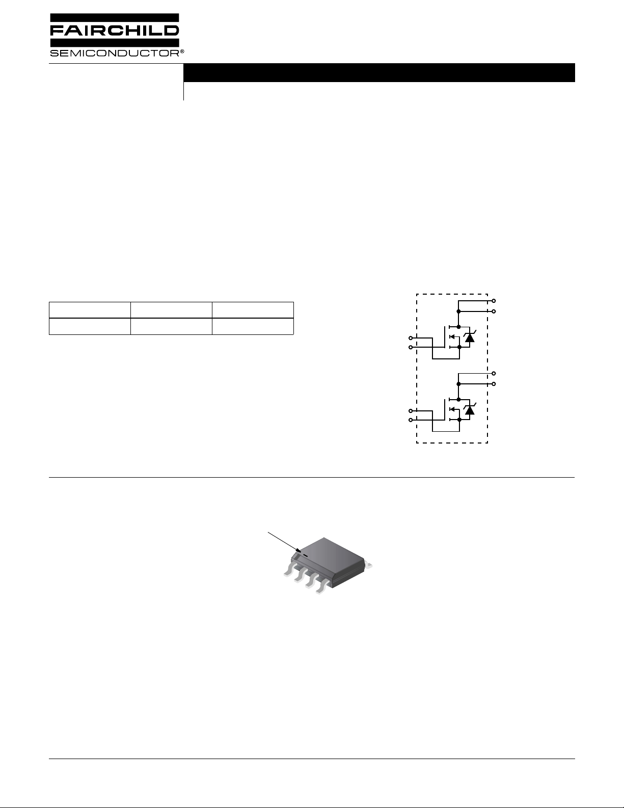
Symbol
D1(8)
D1(7)
S1(1)
G1(2)
D2(6)
D2(5)
S2(3)
G2(4)
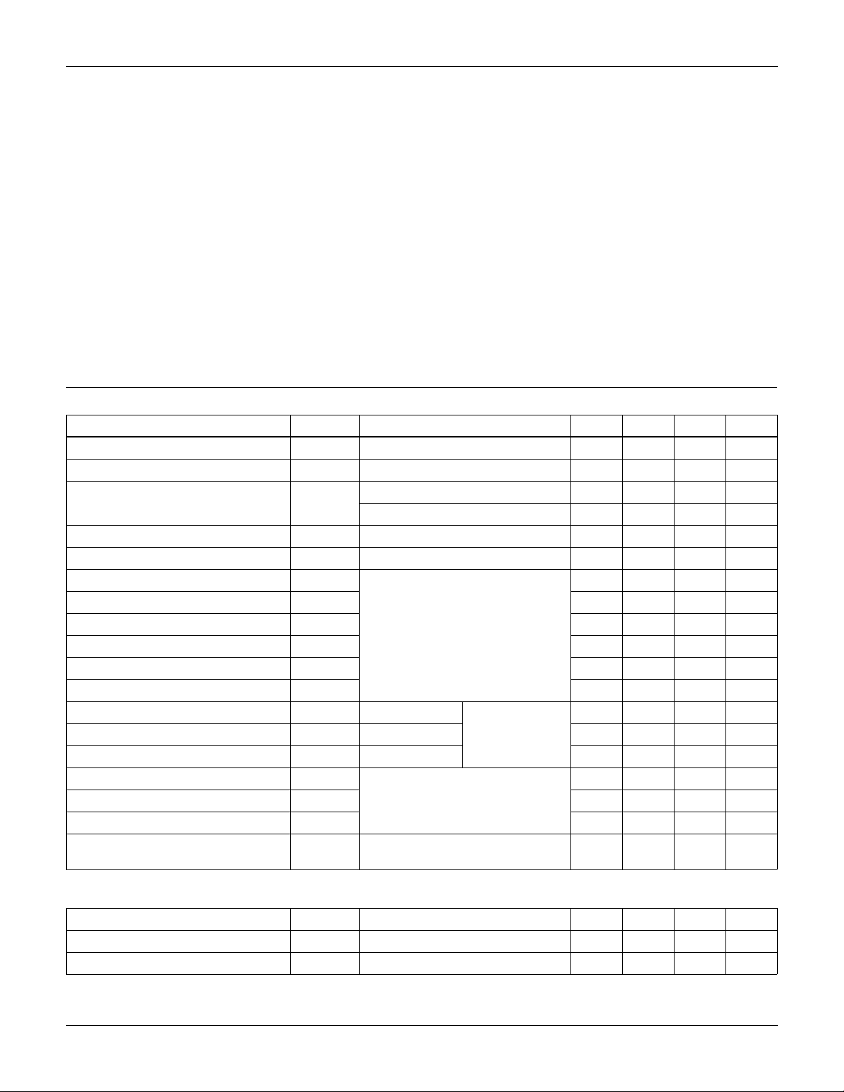
Packaging
JEDEC MS-012AA
BRANDING DASH
5
1
2
3
4
©2002 Fairchild Semiconductor Corpo ration RF1K49154 Rev. B
RF1K49154
Absolute Maximum Ratings
TA = 25oC, Unless Otherwise Specified
RF1K49154 UNITS
Drain to Source Voltage (Note 1). . . . . . . . . . . . . . . . . . . . . . . . . . . . . . . . . . . . . . V
Drain to Gate Voltage (R
= 20kΩ, Note 1). . . . . . . . . . . . . . . . . . . . . . . . . . . . V
GS
Gate to Source Voltage . . . . . . . . . . . . . . . . . . . . . . . . . . . . . . . . . . . . . . . . . . . . . . V
Drain Current Continuous
(Pulse width = 5s) . . . . . . . . . . . . . . . . . . . . . . . . . . . . . . .I
Pulsed (Figure 5) . . . . . . . . . . . . . . . . . . . . . . . . . . . . . . . . . . . . . . . . . . . . . . . . . I
Pulsed Avalanche Rating (Figure 6) . . . . . . . . . . . . . . . . . . . . . . . . . . . . . . . . . . . . E
Power Dissipation . . . . . . . . . . . . . . . . . . . . . . . . . . . . . . . . . . . . . . . . . . . . . . . . . . . P
Derate Above 25oC . . . . . . . . . . . . . . . . . . . . . . . . . . . . . . . . . . . . . . . . . . . . . . . . . .
Operating and Storage Temperature . . . . . . . . . . . . . . . . . . . . . . . . . . . . . . . . T
DSS
DGR
GS
D
DM
AS
D
, T
J
STG
Refer to Peak Current Curve
Maximum Temperature for Soldering
Leads at 0.063in (1.6mm) from Case for 10s. . . . . . . . . . . . . . . . . . . . . . . . . . . . . T
Package Body for 10s, See Techbrief 334 . . . . . . . . . . . . . . . . . . . . . . . . . . . . . T
CAUTION: Stresses above those listed in “A bsolute Maximu m Rating s” may cause per manent d amage to t he device. This is a str ess on ly rating and operation o f the
device at these or any other conditions above those indicated in the operational sections of this specification is not implied.
L
pkg
60 V
60 V
±20 V
2
Refer to UIS Curve
2
0.016
-55 to 150
300
260
A
W
W/oC
o
C
o
C
o
C
NOTE:
= 25oC to 125oC.
1. T
J
Electrical Specifications
TA = 25oC, Unless Otherwise Specified
PARAMETER SYMBOL TEST CONDITIONS MIN TYP MAX UNITS
Drain to Source Breakdown Voltage BV
Gate Threshold Voltage V
GS(TH)VGS
Zero Gate Voltage Drain Current I
Gate to Source Leakage Current I
Drain to Source On Resistance r
DS(ON)ID
Turn-On Time t
Turn-On Delay Time t
d(ON)
Rise Time t
Turn-Off Delay Time t
d(OFF)
Fall Time t
Turn-Off Time t
Total Gate Charge Q
g(TOT)VGS
Gate Charge at 10V Q
Threshold Gate Charge Q
Input Capacitance C
Output Capacitance C
Reverse Transfer Capacitance C
Thermal Resistance Junction to Ambient R
DSSID
DSS
GSS
ON
r
f
OFF
g(10)
g(TH)
ISS
OSS
RSS
θJA
= 250µA, VGS = 0V, (Figure 12) 60 - - V
= VDS, ID = 250µA, (Figure 11) 2 - 4 V
VDS = 55V, VGS = 0V - - 1 µA
= 50V, VGS = 0V, TC = 150oC - - 250 µA
V
DS
VGS = ±20V - - ±10 µA
= 2A, VGS = 10V, (Figures 9, 10) - - 0.130 Ω
VDD = 30V, ID ≈ 2A,
= 15Ω, VGS = 10V,
R
L
= 25Ω
R
GS
(Figure 14)
- - 50 ns
-10-ns
-25-ns
-70-ns
-35-ns
- - 155 ns
= 0V to 20V VDD = 48V,
= 2A,
I
VGS = 0V to 10V - 14 17 nC
VGS = 0V to 2V - 0.8 1.0 nC
D
= 24Ω
R
L
(Figure 14)
VDS = 25V, VGS = 0V,
f = 1MHz (Figure 13)
-2632nC
- 340 - pF
- 140 - pF
-40-pF
Pulse Width = 1s
- - 62.5
o
C/W
Device Mounted on FR-4 Material
Source to Drain Diode Specifications
PARAMETER SYMBOL TEST CONDITIONS MIN TYP MAX UNITS
Source to Drain Diode Voltage V
SD
Reverse Recovery Time t
©2002 Fairchild Semiconductor Corpo ration RF1K49154 Rev. B
ISD = 2A - - 1.5 V
ISD = 2A, dISD/dt = 100A/µs--62ns
rr
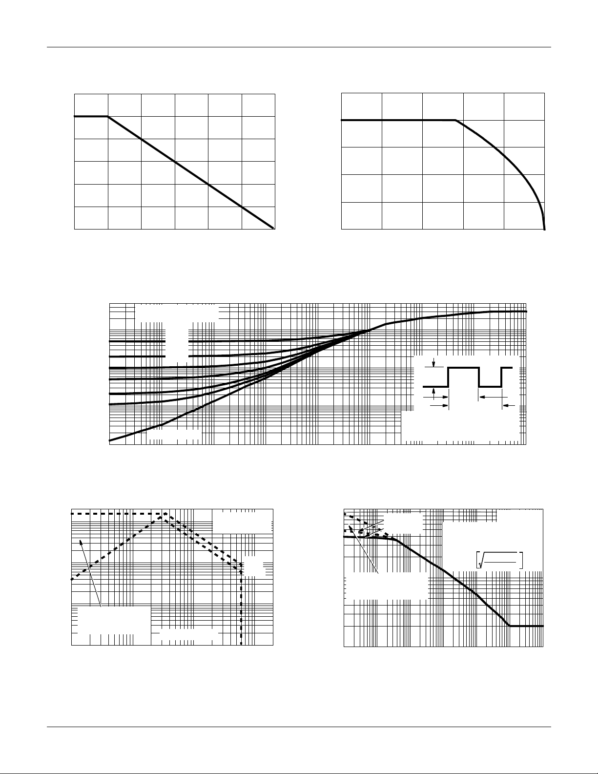
POWER DISSIPATION MULTIPLIER
0
0
I
, DRAIN CURRENT (A)
0
1
I
, PEAK CURRENT CAPABILITY (A)
RF1K49154
Typical Performance Curves
TA = 25oC, Unless Otherwise Specified
1.2
1.0
0.8
0.6
0.4
0.2
0
0 25 50 75 100 15
125
TA, AMBIENT TEMPERATURE (oC)
FIGURE 1. NORMALIZED POWER DISSIPATION vs AMBIENT
TEMPERATURE
, NORMALIZED
Z
θJA
THERMAL IMPEDANCE
0.001
0.1
0.01
5
1
-5
10
DUTY CYCLE
DESCENDING ORDER
0.5
0.2
0.1
0.05
0.02
0.01
SINGLE PULSE
-4
10
-3
10
2.5
2
1.5
1
D
0.5
0
25 50 75 100 125 15
FIGURE 2. MAXIMUM CONTINUOUS DRAIN CURRENT vs
AMBIENT TEMPERATURE
-2
10
t, RECTANGULAR PULSE DURATION (s)
-1
10
0
10
TA, AMBIENT TEMPERATURE (oC)
P
DM
t
1
t
2
NOTES:
DUTY FACTOR: D = t
PEAK TJ = PDM x Z
1
10
θJA
10
1/t2
2
x R
θJA
+ T
A
3
10
FIGURE 3. NORMALIZED MAXIMUM TRANSIENT THERMAL IMPEDANCE
20
10
1
, DRAIN CURRENT (A)
D
OPERATION IN THIS
I
AREA MAY BE
LIMITED BY r
0.1
0.1
TJ = MAX RATED
TA = 25oC
5ms
10ms
DS(ON)
, DRAIN TO SOURCE VOLTAGE (V)
V
DS
V
DSS (MAX)
110 20
= 60V
100
100
10
THERMAL IMPEDANCE
MAY LIMIT CURRENT
IN THIS REGION
DM
1
-5
10
-4
10
= 20V
V
GS
VGS = 10V
-3
10
t, PULSE WIDTH (s)
FOR TEMPERATURES
ABOVE 25
CURRENT AS FOLLOWS:
I
I
=
25
-2
10
10
TA = 25oC
o
C DERATE PEAK
150 - T
A
125
-1
0
10
10
FIGURE 4. FORWARD BIAS SAFE OPERA T ING AREA FIGURE 5. PEAK CURRENT CAPABILITY
©2002 Fairchild Semiconductor Corpo ration RF1K49154 Rev. B
 Loading...