

Fairchild Semiconductor RF1K49086 Datasheet
Power MOSFET Data Sheets
SEMICONDUCTOR
January 1997
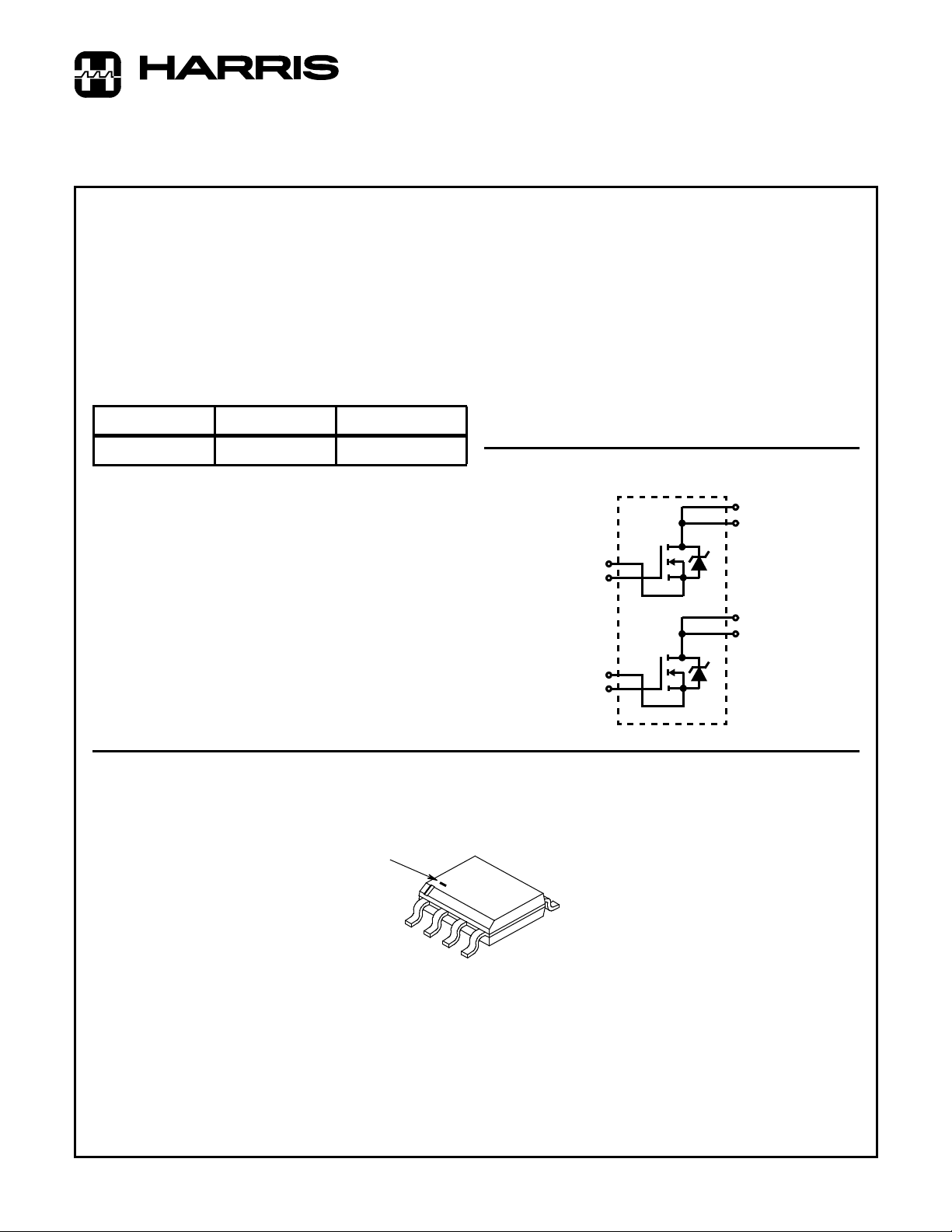
LittleFET™ Enhancement Mode Power MOSFET
Features
• 3.5A, 30V
DS(ON)
= 0.060Ω
PSPICE Model
•r
Temperature Compensating
•
• Peak Current vs Pulse Width Curve
• UIS Rating Curve
Ordering Information
PART NUMBER PACKAGE BRAND
RF1K49086 MS-012AA RF1K49086
NOTE: When ordering, use the entire part number. For ordering in
tape and reel, add the suffix 96 to the part number, i.e. RF1K4908696.
RF1K49086
3.5A, 30V, Avalanche Rated, Dual N-Channel
Description
The RF1K49086 Dual N-Channel power MOSFET is manufactured using an advanced MegaFET process. This process, which uses feature sizes approaching those of LSI
integrated circuits, gives optimum utilization of silicon, resulting in outstanding performance. It is designed for use in
applications such as switching regulators, switching converters, motor drivers, relay drivers, and low voltage bus
switches. This device can be operated directly from integrated circuits.
Formerly developmental type TA49086.
Symbol
D1(8)
D1(7)
Packaging
JEDEC MS-012AA
BRANDING DASH
1
2
S1(1)
G1(2)
D2(6)
D2(5)
S2(3)
G2(4)
5
3
4
LittleFET™ is a trademark of Harris Corporation
CAUTION: These devices are sensitive to electrostatic discharge. Users should follow proper ESD Handling Procedures.
Copyright
© Harris Corporation 1997
5-57
File Number 3986.4
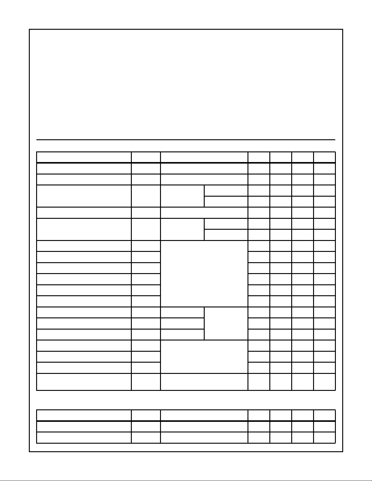
RF1K49086
Absolute Maximum Ratings T
= 25oC Unless Otherwise Specified
A
RF1K49086 UNITS
Drain to Source Voltage . . . . . . . . . . . . . . . . . . . . . . . . . . . . . . . . . . . . . . . . . . . . . . . . . . V
Drain to Gate Voltage. . . . . . . . . . . . . . . . . . . . . . . . . . . . . . . . . . . . . . . . . . . . . . . . . . . . V
Gate to Source Voltage . . . . . . . . . . . . . . . . . . . . . . . . . . . . . . . . . . . . . . . . . . . . . . . . . . . V
DSS
DGR
GS
30 V
30 V
±20 V
Drain Current
Continuous (Pulse Width = 5s). . . . . . . . . . . . . . . . . . . . . . . . . . . . . . . . . . . . . . . . . . . . . . I
Pulsed. . . . . . . . . . . . . . . . . . . . . . . . . . . . . . . . . . . . . . . . . . . . . . . . . . . . . . . . . . . . . . . .I
Pulsed Avalanche Rating . . . . . . . . . . . . . . . . . . . . . . . . . . . . . . . . . . . . . . . . . . . . . . . . . . E
D
Refer to Peak Current Curve
DM
AS
3.5
Refer to UIS Curve
A
Power Dissipation
TA = 25oC . . . . . . . . . . . . . . . . . . . . . . . . . . . . . . . . . . . . . . . . . . . . . . . . . . . . . . . . . . . . . P
D
Derate Above 25oC. . . . . . . . . . . . . . . . . . . . . . . . . . . . . . . . . . . . . . . . . . . . . . . . . . . . . . . . .
Operating and Storage Temperature . . . . . . . . . . . . . . . . . . . . . . . . . . . . . . . . . . . . . T
Soldering Temperature of Leads for 10s . . . . . . . . . . . . . . . . . . . . . . . . . . . . . . . . . . . . . . . .T
CAUTION: Stresses above those listed in “Absolute Maximum Ratings” may cause permanent damage to the device. This is a stress only rating and operation
of the device at these or any other conditions above those indicated in the operational sections of this specification is not implied.
Electrical Specifications T
= 25oC, Unless Otherwise Specified
A
STG
, T
J
L
2
0.016
-55 to 150
260
W
W/oC
o
C
o
C
PARAMETERS SYMBOL TEST CONDITIONS MIN TYP MAX UNITS
Drain to Source Breakdown Voltage BV
Gate Threshold Voltage V
Zero Gate Voltage Drain Current I
DSSID
GS(TH)VGS
DSS
= 250µA, VGS = 0V 30 - - V
= VDS, ID = 250µA1-3V
VDS = 30V,
TA = 25oC--1µA
VGS = 0V
T
= 150oC--50µA
A
Gate to Source Leakage Current I
On Resistance r
Turn-On Time t
GSS
DS(ON)ID
ON
VGS = ±20V - - 100 nA
= 3.5A VGS = 10V - - 0.060 Ω
V
= 4.5V - - 0.132 Ω
GS
VDD = 15V, ID = 3.5A,
- - 50 ns
RL = 4.29Ω, VGS = 10V,
Turn-On Delay Time t
d(ON)
Rise Time t
Turn-Off Delay Time t
d(OFF)
Fall Time t
Turn-Off Time t
Total Gate Charge Q
g(TOT)VGS
RGS = 25Ω
r
f
OFF
= 0V to 20V VDD = 24V,
-10-ns
-30-ns
-60-ns
-45-ns
- - 130 ns
-3545nC
ID = 3.5A,
Gate Charge at 10V Q
Threshold Gate Charge Q
Input Capacitance C
g(10)
g(TH)
ISS
VGS = 0V to 10V - 13 17 nC
RL = 6.86Ω
VGS = 0V to 2V - 2.3 2.9 nC
VDS = 25V, VGS = 0V,
- 575 - pF
f = 1MHz
Output Capacitance C
Reverse Transfer Capacitance C
Thermal Resistance Junction-to-Ambient R
OSS
RSS
θJA
Pulse Width = 1s
- 275 - pF
- 100 - pF
- - 62.5
o
C/W
Device mounted on FR-4 material
Source to Drain Diode Ratings and Specifications
PARAMETERS SYMBOL TEST CONDITIONS MIN TYP MAX UNITS
Forward Voltage V
Reverse Recovery Time t
SD
ISD = 3.5A - - 1.25 V
ISD = 3.5A, dISD/dt = 100A/µs--45ns
rr
5-58
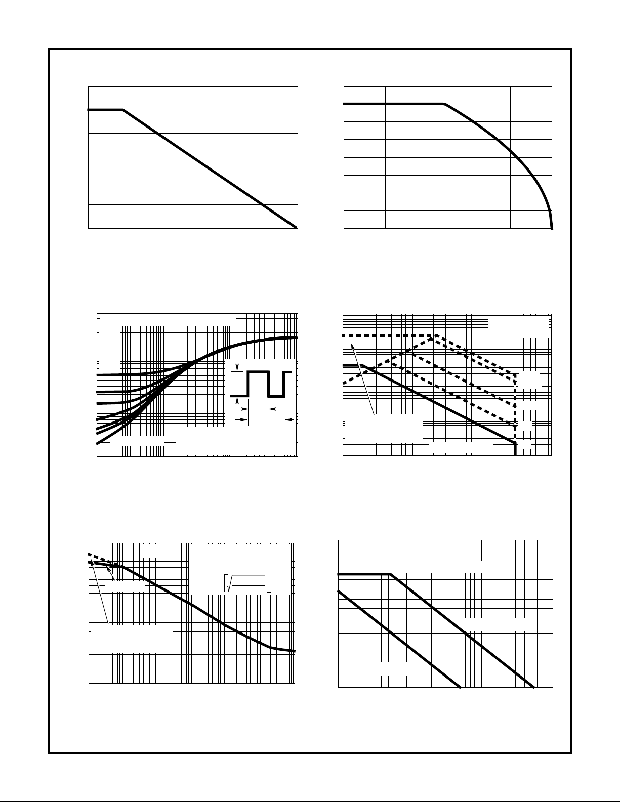
Typical Performance Curves
RF1K49086
1.2
1.0
0.8
0.6
0.4
0.2
POWER DISSIPATION MULTIPLIER
0.0
0 25 50 75 100 150
TA, AMBIENT TEMPERATURE (oC)
FIGURE 1. NORMALIZED POWER DISSIPATION vs
TEMPERATURE DERATING CURVE
10
DUTY CYCLE - DESCENDING ORDER
0.5
0.2
0.1
0.05
0.02
1
0.01
P
DM
, NORMALIZED
JA
0.1
θ
Z
THERMAL IMPEDANCE
NOTES:
DUTY FACTOR: D = t
PEAK TJ = PDM x Z
-1
10
0
10
1/t2
x R
JA
θ
1
10
0.01
SINGLE PULSE
-3
10
-2
10
t, RECTANGULAR PULSE DURATION (s)
125
t
1
10
4.0
3.5
3.0
2.5
2.0
1.5
, DRAIN CURRENT (A)
1.0
D
I
0.5
0.0
25
50
75 100 125 150
TA, AMBIENT TEMPERATURE (oC)
FIGURE 2. MAXIMUM CONTINUOUS DRAIN CURRENT vs
TEMPERA TURE
100
10
1
, DRAIN CURRENT (A)
D
t
2
+ T
JA
A
θ
2
3
10
0.1
OPERATION IN THIS
I
AREA MAY BE
LIMITED BY r
0.01
0.1
DS(ON)
V
DSS
MAX = 30V
1 10 100
VDS, DRAIN-TO-SOURCE VOLTAGE (V)
TJ = MAX RATED
= 25oC
T
A
5ms
10ms
100ms
1s
DC
FIGURE 3. NORMALIZED MAXIMUM TRANSIENT THERMAL
IMPEDANCE
200
100
VGS = 10V
10
TRANSCONDUCTANCE
MAY LIMIT CURRENT
IN THIS REGION
, PEAK CURRENT CAPABILITY (A)
DM
I
1
-5
10
TA = 25oC
-4
10
-3
10
t, PULSE WIDTH (s)
FOR TEMPERATURES
ABOVE 25
o
C DERATE PEAK
CURRENT AS FOLLOWS:
150 - T
I = I
25
-2
10
10
A
125
-1
10
0
FIGURE 5. PEAK CURRENT CAPABILITY NOTE: Refer to Harris Application Notes AN9321 and AN9322.
FIGURE 4. FORWARD BIAS SAFE OPERATING AREA
20
If R = 0
tAV = (L)(IAS)/(1.3*RATED BV
If R ≠ 0
t
= (L/R)ln[(IAS*R)/(1.3*RATED BV
AV
10
DSS
- VDD)
DSS
- VDD) +1]
STARTING TJ = 25oC
, AVALANCHE CURRENT (A)
AS
I
1
10
STARTING TJ = 150oC
1
0.1
1 10 100
tAV, TIME IN AVALANCHE (ms)
FIGURE 6. UNCLAMPED INDUCTIVE SWITCHING CAPABILITY
5-59
 Loading...