

Fairchild Semiconductor RC6334 Datasheet

www.fairchildsemi.com
RC6334
Quad Video Amplifier
Features
• Quad video amplifier
• 175 MHz -3 dB Bandwidth (A
• 50 MHz
• Unity gain stable
• 0.06% differential gain (A
• 0.06
• High CMRR (95dB), High PSRR (80 dB)
• Dual
• Low offset 3.0 mV typical
• 14-pin narrow SO package
• 250V/
• Fast settling time: 0.1% in 15 ns
• TTL or CMOS compatible
±
0.1 dB gain flatness
°
differential phase (A
±
5V power supply
m
s slew rate
= 1, R
V
= 1, R
V
V
= 2)
L
= 150
= 150
L
W
)
W
)
Description
The RC6334 consists of four low power, wide band voltage
feedback operational amplifiers. Each channel is capable of
delivering a load current of at least 35mA.
The amplifiers are optimized for video applications where
low differential gain and low phase distortion are significant
requirements.
Applications
• RGB amplifiers
• Video instrumentation amplifier
• Selectable gain amplifier
• Active filters
• Set-top box Buffers/Drivers
Block Diagram
RC6334
OUT4
IN4–
IN4+
V
CC
IN1+
IN1–
–
+
+
–
OUT2
IN2–
–
+
IN2+
V
EE
IN3+
+
–
IN3–
OUT1 OUT3
65-3527-01
Rev. 1.0.1
1
PRODUCT SPECIFICATION RC6334
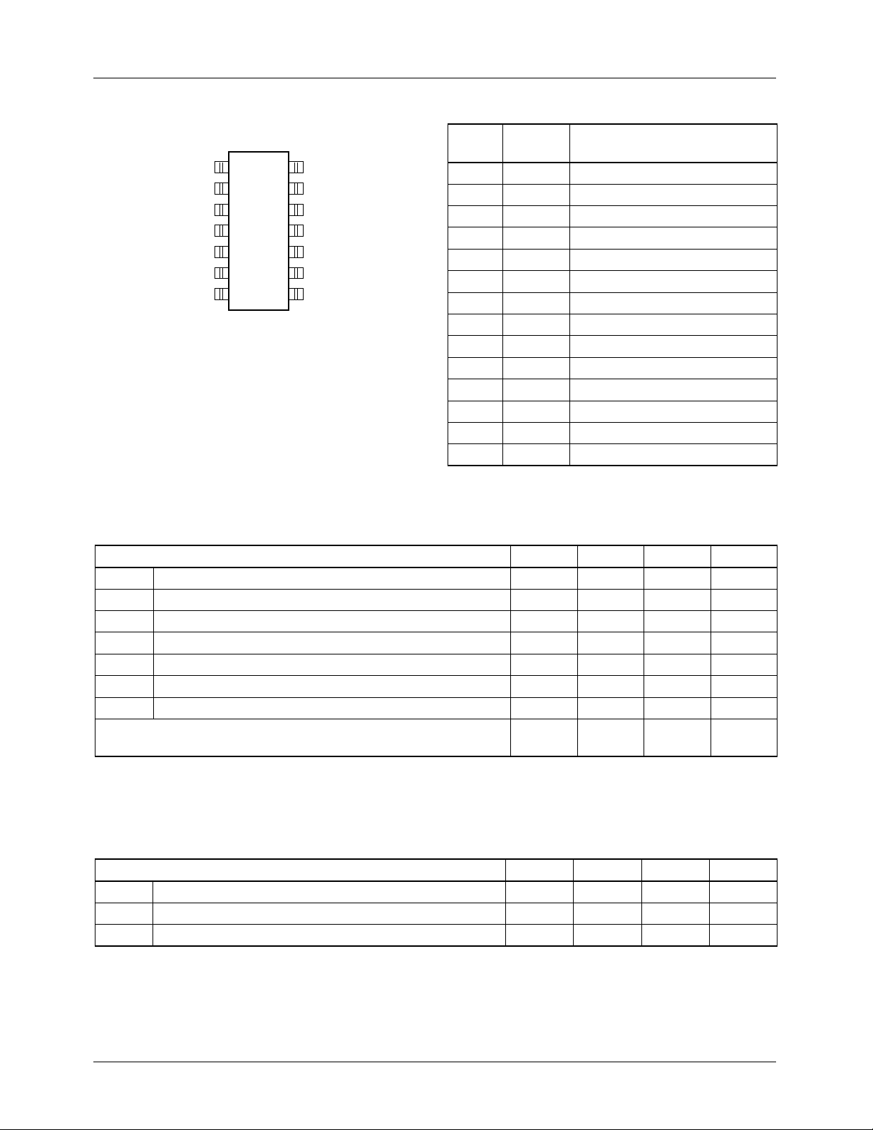
Pin Assignments
RC6334
OUT4
IN4–
IN4+
V
IN1+
IN1–
OUT1
CC
1
2
3
4
5
6
7
14
13
12
11
10
65-3527-02
OUT2
IN2–
IN2+
V
EE
IN3+
IN3–
9
OUT3
8
Pin Definitions
Pin
Name
IN1– 6 Amplifier 1 inverting input
IN1+ 5 Amplifier 1 non-inverting input
IN2– 13 Amplifier 2 inverting input
IN2+ 12 Amplifier 2 non-inverting input
IN3– 9 Amplifier 3 inverting input
IN3+ 10 Amplifier 3 non-inverting input
IN4– 2 Amplifier 4 inverting input
IN4+ 3 Amplifier 4 non-inverting input
Pin
Number
Pin Function Description
OUT1 7 Amplifier 1 output
OUT2 14 Amplifier 2 output
OUT3 8 Amplifier 3 output
OUT4 1 Amplifier 4 output
V
CC
V
EE
4 Analog positive supply
11 Analog negative supply
Absolute Maximum Ratings
(beyond which the device may be damaged)
Parameter Min Typ Max Units
V
CC
V
EE
Short circuit tolerance:
No more than one output can be shorted to ground.
Notes:
1. Functional operation under any of these conditions is NOT implied.
Positive power supply 7 V
Negative power supply -7 V
Differential input voltage 10 V
Operating Temperature 0 +70
Storage Temperature -40
±
125
Junction Temperature 150
Lead Soldering (10 seconds) 240
°
C
°
C
°
C
°
C
Operating Conditions
Parameter Min Typ Max Units
V
CC
V
EE
q
JA
2
Power Supply Voltage 4.75 5.0 5.25 V
Negative Supply Voltage -4.75 -5.0 -5.25 V
SO14 Thermal Resistance 105
°
C/W
W
RC6334 PRODUCT SPECIFICATION
DC Characteristics
W
V
CC
= 5V, V
= -5V, A
EE
= 2, R
V
LOAD
= 150
, T
Parameter Conditions Min Typ Max Units
V
OS
D
V
OS
I
B
/
D
I
B
Rin Input Resistance
Cin Input Capacitance
Input Offset Voltage No Load 3
/
D
T Offset Voltage Drift
1
Input Bias Current
D
T Input Bias Current Drift
1
1
1
CMIR Common Mode Input Range
CMRR Common Mode Rejection Ratio No Load 70 100 dB
PSRR Power Supply Rejection Ratio No Load 65 80 dB
Is Quiescent Supply Current No Load 33 48 mA
R
OUT
I
OUT
V
OUT
A
VOL
Note:
1. Guaranteed by design.
Output Impedance (Closed Loop)
Output Current Per Amplifier 35 mA
Output Voltage Swing No Load
Open-loop Gain 60 75 dB
°
A
= 0
C to 70
°
C, unless otherwise specified. Open Loop.
±
10 mV
±
6
±
1
±
8
±
30
±
5
±
40 nA/
1M
m
V/
°
C
m
A
°
C
W
0.5 2 pF
±
2.5 V
1
Enabled, At DC 0.2
±
R
L
= 150
2.5
±
2.5
±
3.0 V
±
3.0 V
W
AC Characteristics
°
V
CC
= 5V, V
= -5V, A
EE
= 2, T
V
= 0 to 70
A
C, R
LOAD
specified. Closed Loop. Guaranteed by Design. See Typical Test Circuit.
Parameter Conditions Min Typ Max Units
Frequency Response
BW -3 dB Bandwidth (A
Flat
±
0.1 dB Bandwidth V
Peak Maximum Small Signal AC Peaking V
X
TALK
Crosstalk Isolation @ 5 MHz 50 dB
= 2) V
V
V
OUT
OUT
OUT
OUT
Time Domain Response
t
, t
r1
Rise and Fall Time 10% to 90% 2V Output Step 10 15 ns
f1
ts Settling Time to 0.1% 2V Output Step 15 ns
OS Overshoot 2V Output Step 5 %
US Undershoot 2V Output Step 2 %
SR Slew Rate V
OUT
Distortion
HD
HD
2nd Harmonic Dist. @ 20 MHz V
2
3nd Harmonic Dist. @ 20 MHz V
3
OUT
OUT
Video Performance
DG Diff. Gain (p-p), NTSC & PAL RL = 150W, V
DP Diff. Phase (p-p), NTSC & PAL RL = 150W, V
NF Noise Floor >100kHz -130 dB rms
W
= 150
, R
G
= R
F
= 250
W
, C
= 10 pF, unless otherwise
L
= 0.4 Vpp +175 MHz
= 0.8 Vpp 75 90 MHz
= 0.4 Vpp 50 60 MHz
= 0.8 Vpp 0.01 dB
= ±2.0V 200 250 V/ms
= 0.8 Vpp -48 dB
= 0.8 Vpp -56 dB
= ±1.5V 0.06 %
OUT
= ±1.5V 0.06 Deg.
OUT
3
 Loading...