

Fairchild Semiconductor RC5060 Datasheet
www.fairchildsemi.com
RC5060
ACPI Switch Controller
Features
¥ Implements ACPI control with PWROK, SLP_S3# and
SLP_S5 #
¥ Switch and linear regulator controller for 3.3V Dual (PCI)
¥ Linear regulator controller and linear regulator for 2.5V
Dual (RAMBUS)
¥ Two switch controller for 5V Dual (USB)
¥ Switch controller and linear regulator for 3.3V SDRAM
¥ Provides SDRAM and RAMBUS power simultaneously
¥ Adaptive Break-before-Make
¥ Integrated Power Good
¥ Drives all N-Channel MOSFETs plus NPN
¥ Latched overcurrent protection for outputs
¥ Power-up softstarts for the linear regulators
¥ UVLO guarantees correct operation for all conditions
¥ 20 pin SOIC package
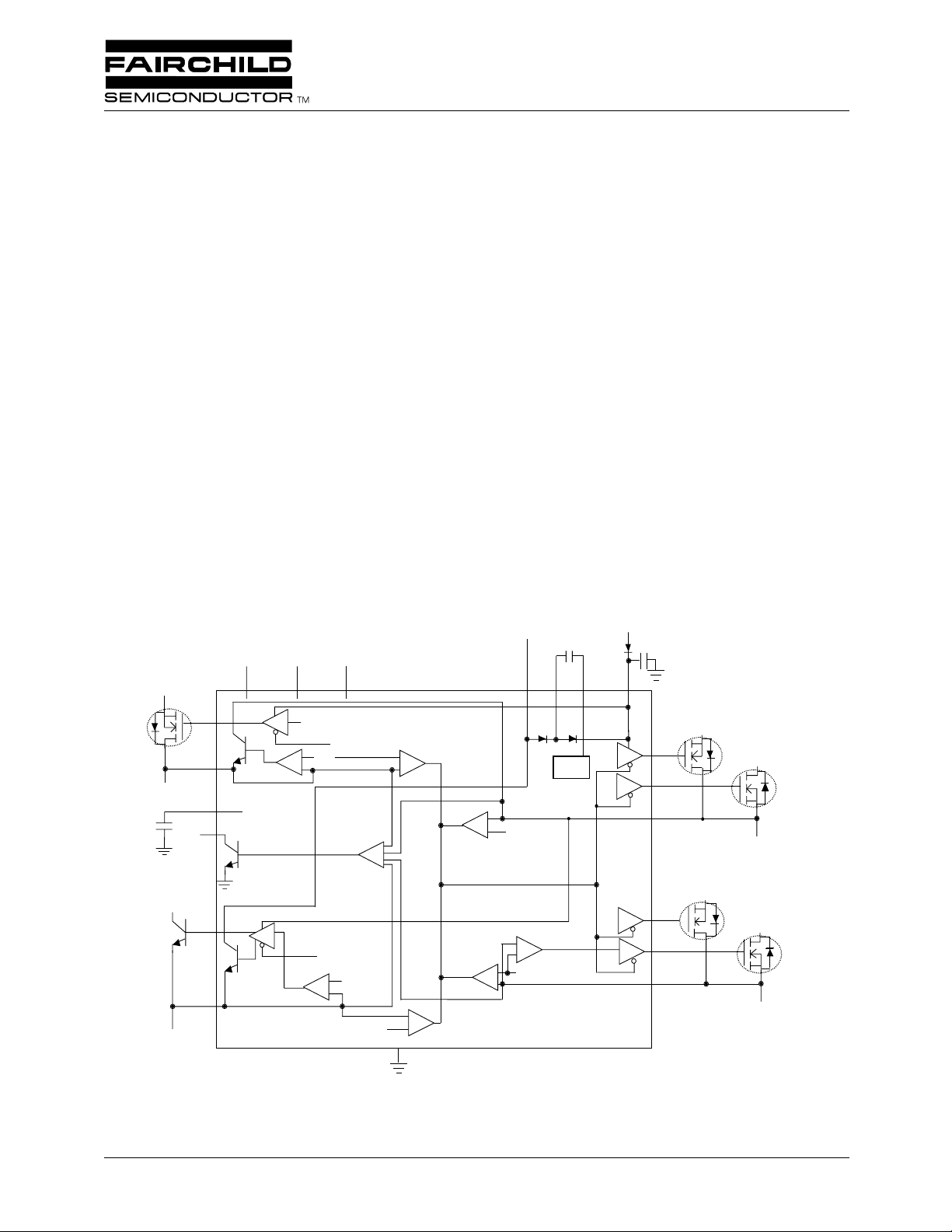
Block Diagram
3.3V Main
3.3V SDRAM
3
4
13
9
PWROK
12
Softstart
PWRGD
SLP_S3#
10
+
-
SLP_S5#
Over Current
Ref
11
+
-
Applications
¥ Camino Platform ACPI Controller
¥ Whitney Platform ACPI Controller
¥ Tehama Platform ACPI Controller
Description
The RC5060 is an ACPI Switch Controller for the Camino,
Whitney and Tehama Platforms. It is controlled by PWROK,
SLP_S3# and SLP_S5#, and provides 3.3V Dual for PCI, 3.3V
for SDRAM, 2.5V Dual for RAMBUS, and 5V Dual voltages.
An on-board precision low TC reference achieves tight tolerance voltage regulation without expensive external components.
The RC5060 also offers integrated Power Good and Current
Limiting that protects each output, and softstart for the linear
regulators. The RC5060 is available in a 20 pin SOIC.
+5V Standby
-
+
REF
521
Osc
+12V
20
+5V Main
19
18
17
+5V Standby
+5V Dual (USB)
3.3V MAIN
2.5V Dual
(
RAMBUS
Over Current
+3.3V Main
16
-
Over Current
REF
+
15
)
-
+
REF
14
+
REF
+
-
6
7
8
+5V Standby
+3.3V Dual (PCI)
REV. 1.0.2 9/14/01
2
RC5060 PRODUCT SPECIFICATION
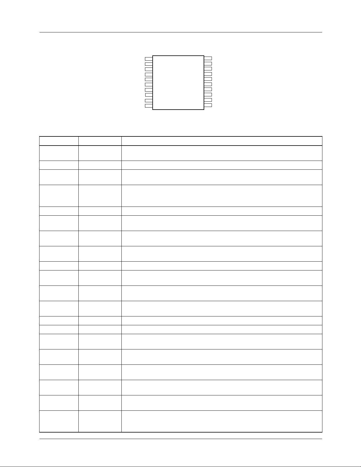
Pin Assignments
QCAP
PUMP
SDRAMOUT
SDRAMFB
5VSTBY
3VOUT1
3VOUT2
3VFB
PWRGD
SLP_S3#
1
2
3
4
5
6
7
8
9
10
RC5060
20
19
18
17
16
15
14
13
12
11
VCCP
5VOUT1
5VOUT2
5VFB
RAMBUSOUT
RAMBUSFB
GND
SS
PWROK
SLP_S5#
Pin Definitions
Pin Number Pin Name Pin Function Description
1 QCAP
2 PUMP
3 SDRAMOUT 3.3V SDRAM gate control. Attach this pin to a transistor powering 3.3V SDRAM
4 SDRAMFB
5 5VSTBY
6 3VOUT1
7 3VOUT2
8 3VFB
9 PWRGD
10 SLP_S3#
11 SLP_S5#
12 PWROK
13 SS
14 GND
15 RAMBUSFB
16 RAMBUSOUT 2.5V base drive control. Attach this pin to an NPN transistor powering 2.5V dual
17 5VFB
18 5VOUT2
19 5VOUT1
20 VCCP
Charge pump cap. Attach flying capacitor between this pin and PUMP to
generate high voltage from standby power.
Charge pump switcher.
from the 3.3V main supply.
3.3V SDRAM voltage feedback. Pin 4 is used as the input for the voltage
feedback control loop for 3.3V SDRAM, and also sources 3.3V SDRAM in
standby.
5V Standby. Apply +5V standby on this pin to run the circuit in standby mode.
3.3V main gate control. Attach this pin to a transistor powering 3.3V dual from
the 3.3V main supply.
3.3V standby gate control. Attach this pin to a transistor powering 3.3V dual
from the 5V standby supply.
3.3V voltage Feedback. Pin 8 is used as the input for the voltage feedback
control loop for 3.3V dual.
Power Good. Open collector output is high when all outputs are valid.
SLP_S3#. Control signal governing the Soft Off state S3. Internal current source
pulls this line high if left open.
SLP_S5#. Control signal governing the Soft Off state S5. Internal current source
pulls this line high if left open.
PWROK. Control signal for switches. Internal current source pulls this line high if left
open.
Softstart. Attach a capacitor to this pin to determine the softstart rate.
Ground. Connect this pin to ground.
2.5V feedback. Pin 15 is used as the input for the voltage feedback control loop for
2.5V dual (RAMBUS), and also sources 2.5V dual in standby.
(RAMBUS) from the 3.3V main supply.
5V Voltage Feedback. Pin 17 is used to sense undervoltage to protect the 5V dual
from overcurrent.
5V standby gate control. Attach this pin to a transistor powering 5V dual from the
5V standby supply.
5V main gate control. Attach this pin to a transistor powering 5V dual from the 5V
main supply.
Main Power. Apply +12V through a diode on this pin to run the circuit in normal
mode. Bypass with a 0.1µF capacitor. When 12V is not present, this pin produces
voltage doubled 5V standby.
REV. 1.0.2 9/14/01
PRODUCT SPECIFICATION RC5060
Absolute Maximum Ratings
VCCP 15V
All Other Pins 13.5V
Junction Temperature, T
J
150°C
Storage Temperature -65 to 150°C
Lead Soldering Temperature, 10 seconds 300°C
Thermal Resistance Junction to Ambient Θ
Thermal Resistance Junction-to-case, Θ
JC
JA
85°C/W
24°C/W
Recommended Operating Conditions
Parameter Conditions Min. Typ. Max. Units
+3.3VMAIN 3.135 3.3 3.465 V
+5VMAIN 4.75 5 5.25 V
+5VSTBY 4.75 5 5.25 V
+12V 11.4 12 12.6 V
Ambient Operating Temperature 0 70 °C
REV. 1.0.2 9/14/01
3
4
RC5060 PRODUCT SPECIFICATION
Electrical Specifications
(V
+5VSTBY
The • denotes specifications which apply over the full operating temperature range.
Parameter Conditions Min. Typ. Max. Units
+5V DUAL
V
Out1
V
Out1
V
GS
V
Out2
Maximum Drive Current, Each • 10 mA
Overcurrent Limit: Undervoltage 80 %V
Overcurrent Delay Time 150 µsec
Output Driver Overlap Time See Figure 2 • 1 5 µsec
+3.3V DUAL
V
Out1
V
Out1
V
Out2
Total Output Voltage Variation
Maximum Drive Current 3VOUT1 On • 90 mA
Minimum Load Current 3VOUT2 On • 50 mA
Overcurrent Limit: Undervoltage 80 %Vout
Overcurrent Delay Time 150 µsec
Output Driver Deadtime See Figure 2: Main → Standby • 2 6 µsec
+2.5V DUAL
I
B
I
Out
Total Output Voltage Variation
Overcurrent Limit 80 %Vout
Overcurrent Delay Time 150 µsec
Output Driver Overlap Time See Figure 2 • 1 5 µsec
+3.3V SDRAM
V
out
V
out
I
Out
Overcurrent Limit 80 %Vout
Total Output Voltage Variation
Overcurrent Delay Time 150 µsec
Output Driver Dead Time • 200 1500 nsec
Common Functions
PWRGD Threshold 80 %Vout
PWRGD Delay Time 150 µsec
PWRGD Sink Current • 1 mA
Charge Pump Frequency 250 KHz
+5VSTBY UVLO 4.5 V
= V
+5VMAIN
=5V, V
+3.3V
= 3.3V, V
= 12V and T
+12V
= +25°C using circuit in Figure 4, unless otherwise noted.)
A
, On • 10 V
, Off I = 10µA • 200 mV
,
Out2
Standby • 2.7 V
, Off I = 10µA • 200 mV
, On • 10 V
, Off I = 10µA • 200 mV
, On Standby • 5 mA
1
3VOUT2 On • 3.135 3.3 3.465 V
: Standby → Main • 200 1000 nsec
, On RAMBUSOUT On • 200 mA
RAMBUSOUT Off • 144 mA
1
• 2.375 2.5 2.625 V
, On • 10 V
, Off I = 10µA • 200 mV
SDRAMOUT Off • 100 mA
1
SDRAMFB On • 3.135 3.3 3.465 V
out
REV. 1.0.2 9/14/01
PRODUCT SPECIFICATION RC5060
→
Electrical Specifications (continued)
(V
+5VSTBY
The • denotes specifications which apply over the full operating temperature range.
Parameter Conditions Min. Typ. Max. Units
+5VSTBY UVLO Hysteresis 0.5 V
+12V UVLO 7.5 V
+12V UVLO Hysteresis 1 V
+5VSTBY Current MAIN Power Present 10 25 mA
+12V Current 2.5 10 mA
Input Logic HIGH • 2.0 V
Input Logic LOW • 0.8 V
Softstart Current 3 6 9 µA
Control Line Input Current SLP_S5#, SLP_S3#, PWROK • 10 µA
Over Temperature Shutdown 150 °C
Note:
1. Voltage Regulation includes Initial Voltage Setpoint and Output Temperature Drift.
= V
+5VMAIN
=5V, V
+3.3V
= 3.3V, V
= 12V and T
+12V
= +25°C using circuit in Figure 4, unless otherwise noted.)
A
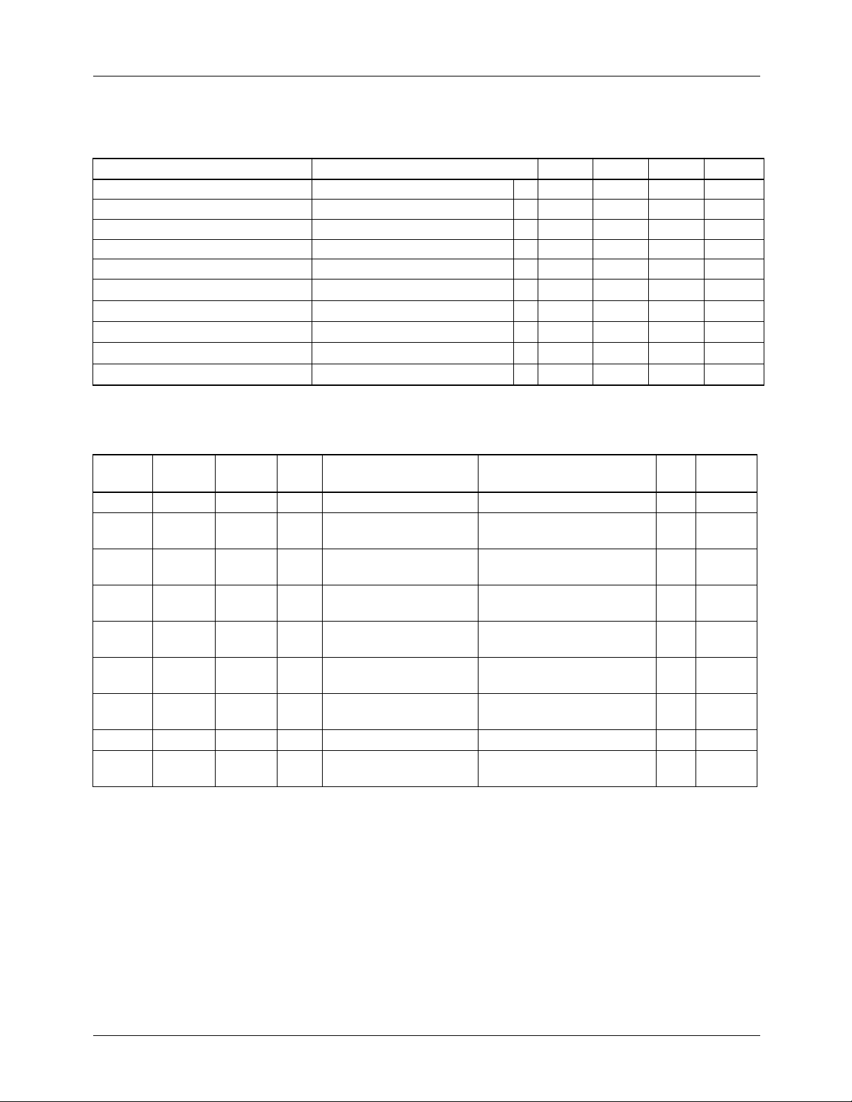
Table 1. Power Descriptors
2.5V RAMBUS/
PWROK SLP_S3# SLP_S5# Main 5V/3.3V Duals
1 1 1 ON ON, Powered from MAIN ON, Powered from MAIN S0 S0
1 0 1 OFF ON, Powered from
STANDBY
0 0 1 OFF ON, Powered from
STANDBY
0 1 1 OFF ON, Powered from
STANDBY
1 0 0 OFF ON, Powered from
STANDBY
0 0 0 OFF ON, Powered from
STANDBY
0 1 0 OFF ON, Powered from
STANDBY
1 1 0 ON ON, Powered from MAIN OFF S5 Not Used
000
1 OFF ON, Powered from
STANDBY
*When PWROK = SLP_S3# = 0 and SLP_S5# transitions from 0 to 1, the RC5060 remains in the S5 state. See Table 2.
3.3V SDRAM State Usage
ON, Powered from
S3 S0 → S3
STANDBY
ON, Powered from
S3 S3
STANDBY
ON, Powered from
S3 S3 → S0
STANDBY
OFF S5 S0 → S5
OFF S5 S5
OFF S5 S5 → S0
OFF S5* *
REV. 1.0.2 9/14/01
5
 Loading...