

Fairchild Semiconductor RC5058 Datasheet
www.fairchildsemi.com
RC5058
High Performance Programmable Synchronous
DC-DC Controller for Multi-Voltage Platforms
Features
•P rogrammable output for Vcore from 1.3V to 3.5V using
an integrated 5-bit DAC
Controls adjustable linears for Vagp (selectable 1.5V/3.3V),
•
Vclock (2.5V), and Vtt (1.5V) or Vnorthbridge (1.8V)
• Meets VRM specification with as few as 5 capacitors
• Meets 1.550V +40/-70mV over initial tolerance,
temperature and transients
• Remote sense
• Programmable Active Droop™ (Voltage Positioning)
• Drives N-Channel MOSFETs
• Overcurrent protection using MOSFET sensing
• 85% efficiency typical at full load
• Integrated Power Good and Enable/Soft Start functions
• 24 pin SOIC package
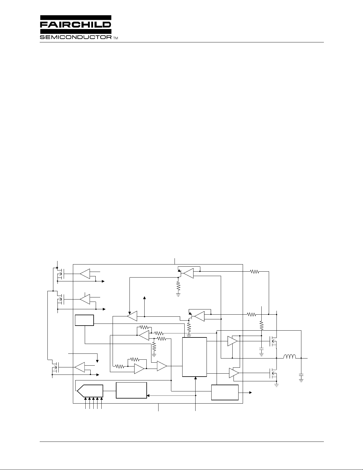
Block Diagram
+3.3V
+1.5V
+2.5V
9
+
10
VCCP
11
+
12
OSC
REF
PWRGD,
OCL
REF
-
PWRGD,
OCL
OCL
VCCA
-
+
Applications
• Power supply for Pentium
• Power supply for Pentium III Whitney Platform
• VRM for Pentium III processor
• Programmable multi-output power supply
®
III Camino Platform
Description
The RC5058 is a synchronous mode DC-DC controller IC
which provides a highly accurate, programmable set of output
voltages for multi-voltage platforms such as the Intel Camino,
and provides a complete solution for the Intel Whitney and other
high-performance processors. The RC5058 features remote
voltage sensing, independently adjustable current limit, and a
proprietary Programmable Active Droop
transient response. The RC5058 uses a 5-bit D/A converter
to program the output voltage from 1.3V to 3.5V. The RC5058
uses a high level of integration to deliver load currents in excess
+5V
21
-
+
-
+
19
18
20
24
1
R
R
S
VCCP
HIDRV
D
+12V
™
for optimal converter
+5V
15
14
+
V
-
5-Bit
DAC
VID2
PWRGD, OCL
VID4
VID3
3.3/1.5V
Pentium is a registered trademark of Intel Corporation. Programmable Active Droop is a trademark of Fairchild Semiconductor.
13
87654
VID0
VID1
-
+
1.24V
Reference
-
+
3
GNDA
Digital
Control
16
ENABLE/SS
Power
Good
2
23
22
17
LODRV
GNDP
PWRGD
VCC
Rev. 1.0.0
2
RC5058 PRODUCT SPECIFICATION
of 16A from a 5V source with minimal external circuitry.
Synchronous-mode operation offers optimum efficiency over
the entire specified output voltage range. An on-board precision
low TC reference achieves tight tolerance voltage regulation
without expensive external components, while Programmable
Active Droop
™
permits exact tailoring of voltage for the most
demanding load transients. The RC5058 includes linear regulator
controllers for Vtt termination (1.5V), Vclock (2.5V), and
Vnorthbridge (1.8V) or Vagp (selectable 1.5V/3.3V), each adjustable with an external divider. The RC5058 also offers integrated
functions including Power Good, Output Enable/Soft Start and
current limiting, and is available in a 24 pin SOIC package.
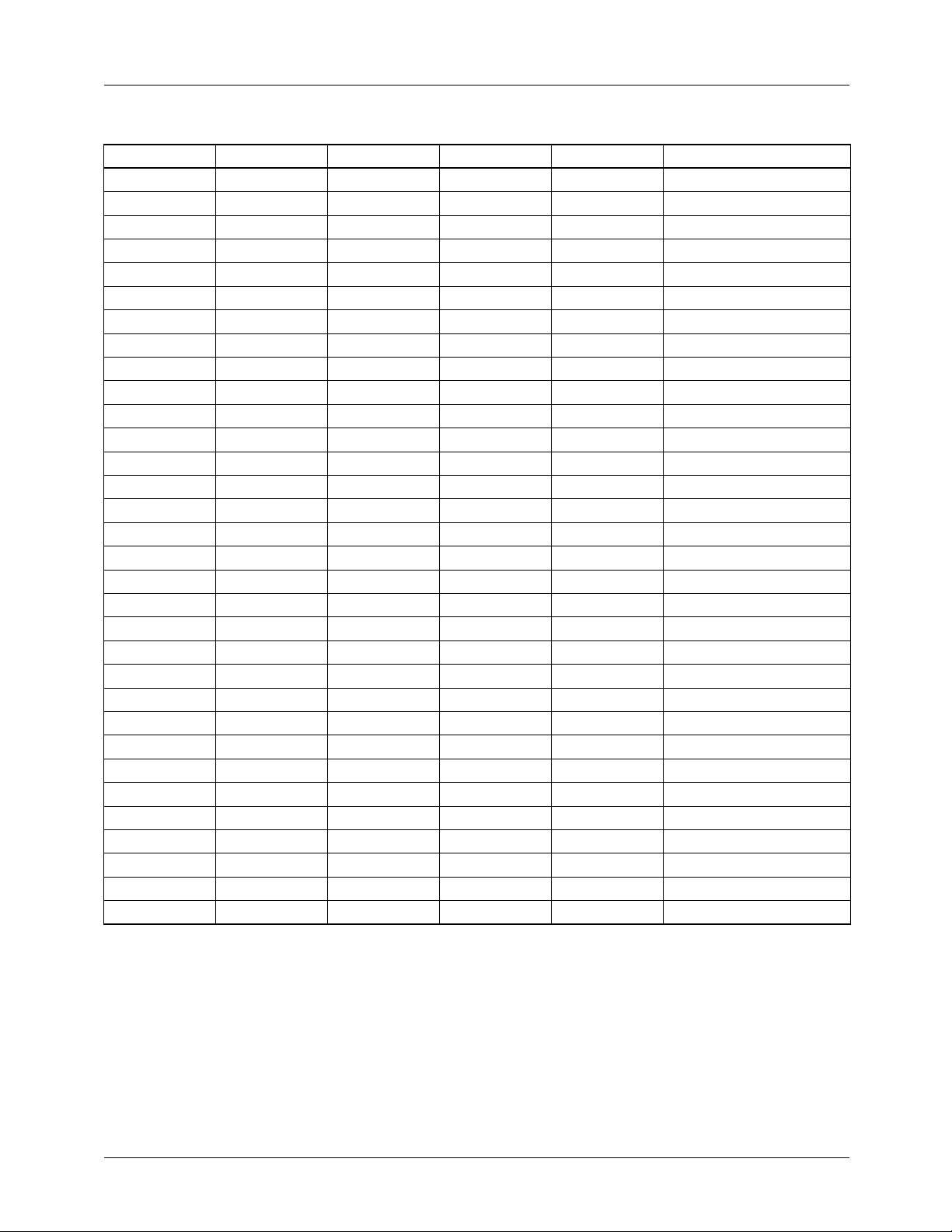
Pin Definitions
Pin
Number Pin Name Pin Function Description
1 HIDRV
2SW
3 GNDA
4-8 VID0-4
9 VTTGATE Gate Driver for VTT Transistor. For 1.5V output.
10 VTTFB
11 VCKGATE Gate Driver for VCK Transistor. For 2.5V output.
12 VCKFB
13 VAGPFB
14 VAGPGATE Gate Driver for VAGP Transistor. For 3.3/1.5V output.
15 TYPEDET Type Detect. Sets 3.3V or 1.5V for AGP.
16 ENABLE/SS Output Enable. A logic LOW on this pin will disable all outputs. An internal current source
17 PWRGD
18 ILIM
19 DROOP
20 VFB
21 VCCA
22 GNDP
23 LODRV
24 VCCP
High Side FET Driver. Connect this pin through a resistor to the gate of an N-channel
MOSFET. The trace from this pin to the MOSFET gate should be <0.5".
High side Driver Source and Low side Driver Drain Switching Node. Together with
DROOP and ILIM pins allows FET sensing for Vcc current.
Analog Ground. Return path for low power analog circuitry. This pin should be
connected to a low impedance system ground plane to minimize ground loops.
Voltage Identification Code Inputs. These open collector/TTL compatible inputs will
program the output voltage over the ranges specified in Table 2. Pull-up resistors are
internal to the controller.
Voltage Feedback for VTT.
Voltage Feedback for VCK.
Voltage Feedback for VAGP.
allows for open collector control. This pin also doubles as soft start for all outputs.
Power Good Flag. An open collector output that will be logic LOW if any output voltage
is more than ±12% outside of the nominal output voltage setpoint.
Vcc Current Feedback. Pin 18 is used in conjunction with pin 2 as the input for the Vcc
current feedback control loop. Layout of these traces is critical to system performance.
See Application Information for details.
Droop set. Use this pin to set magnitude of active droop.
Vcc Voltage Feedback. Pin 20 is used as the input for the Vcc voltage feedback control
loop. See Application Information for details regarding correct layout.
Analog VCC. Connect to system 5V supply and decouple with a 0.1µF ceramic capacitor.
Power Ground. Return pin for high currents flowing in pin 24 (VCCP).
Vcc Low Side FET Driver. Connect this pin through a resistor to the gate of an N-channel
MOSFET for synchronous operation. The trace from this pin to the MOSFET gate should
be <0.5".
Power VCC. For all FET drivers. Connect to system 12V supply through a 33 Ω , and
decouple with a 1µF ceramic capacitor.
Pin Assignments
HIDRV
SW
GNDA
VID4
VID3
VID2
VID1
VID0
VTTGATE
VTTFB
VCKGATE
VCKFB
1
2
3
4
5
6
7
8
9
10
11
12
RC5058
24
23
22
21
20
19
18
17
16
15
14
13
VCCP
LODRV
GNDP
VCCA
VFB
DROOP
ILIM
PWRGD
SS/ENABLE
TYPEDET
VAGPGATE
VAGPFB
REV. 1.0.0 6/30/00
PRODUCT SPECIFICATION RC5058
Absolute Maximum Ratings
Supply Voltage VCCA to GND 13.5V
Supply Voltage VCCP to GND 15V
Voltage Identification Code Inputs, VID0-VID4 VCCA
All Other Pins 13.5V
Junction Temperature, T
J
150°C
Storage Temperature -65 to 150°C
Lead Soldering Temperature, 10 seconds 300°C
Thermal Resistance Junction-to-ambient, Θ
Note:
1. Component mounted on demo board in free air.
JA
1
75°C/W
Recommended Operating Conditions
Parameter Conditions Min. Typ. Max. Units
Supply Voltage VCCA 4.5 5 5.25 V
Input Logic HIGH 2.0 V
Input Logic LOW 0.8 V
Ambient Operating Temperature 0 70 °C
Output Driver Supply, VCCP 10.8 12 13.2 V
Electrical Specifications
(V
= 5V, V
CCA
The • denotes specifications which apply over the full operating temperature range.
Parameter Conditions Min. Typ. Max. Units
VCC Regulator
Output Voltage See Table 1 • 1.3 3.5 V
Output Current 18 A
Initial Voltage Setpoint I
Output Temperature Drift T
Line Regulation V
Internal Droop Impedance I
Maximum Droop 60 mV
Output Ripple 20MHz BW, I
Total Output Variation,
Steady State
Total Output Variation,
Transient
Short Circuit Detect Current • 45 50 60 µA
Efficiency I
Output Driver Rise & Fall Time See Figure 3 50 nsec
Output Driver Deadtime See Figure 3 50 nsec
CCP
2
= 12V, V
1
= 2.0V, and T
OUT
= +25°C using circuit in Figure 1 unless otherwise noted.)
A
= 0.8A,V
LOAD
= 0 to 70°C,V
A
= 4.75V to 5.25V • -4 mV/V
IN
= 0.8A to 12.5A 13.0 14.4 15.8 K Ω
LOAD
V
= 2.000V
OUT
V
= 1.550V
OUT
I
= 0.8A to 18A, V
LOAD
= 18A, V
LOAD
= 2.400V
OUT
V
= 2.000V
OUT
V
= 1.550V
OUT
= 2.000V
OUT
V
= 1.550V
OUT
= 18A 11 mVpk
LOAD
3
= 2.000V
OUT
V
= 1.550V
OUT
= 2.0V 85 %
OUT
3
2.397
2.000
1.550
•
•
••1.940
1.480
••1.900
1.480
2.424
2.020
1.565
+8
+6
2.454
2.040
1.580
2.070
1.590
2.100
1.590
V
V
V
mV
mV
V
V
REV. 1.0.0 6/30/00
3
4
≤
≤
≤
≤
RC5058 PRODUCT SPECIFICATION
Electrical Specifications
(V
CCA
= 5V, V
CCP
= 12V, V
OUT
(Continued)
= 2.0V, and T
= +25°C using circuit in Figure 1 unless otherwise noted.)
A
The • denotes specifications which apply over the full operating temperature range.
Parameter Conditions Min. Typ. Max. Units
Duty Cycle 0 100 %
5V UVLO • 3.74 4 4.26 V
12V UVLO • 7.65 8.5 9.35 V
Soft Start Current • 5 10 17 µA
VTT Linear Regulator
Output Voltage I
2A • 1.455 1.5 1.545 V
LOAD
Under Voltage Trip Level Over Current 80 %V
VCLK Linear Regulator
Output Voltage I
2A • 2.375 2.5 2.625 V
LOAD
Under Voltage Trip Level Over Current 80 %V
VAGP Linear Regulator
Output Voltage I
Output Voltage I
2A, TYPEDET=0V • 1.425 1.5 1.575 V
LOAD
2A, TYPEDET=OPEN • 3.135 3.3 3.465 V
LOAD
Under Voltage Trip Level Over Current 80 %V
Common Functions
Oscillator Frequency • 255 310 345 kHz
PWRGD Threshold Logic HIGH, All Outputs
Linear Regulator Under Voltage
Logic LOW, Any Output
Over Current 30 µsec
•
92
•
88
108
112
Delay Time
Notes:
1. Steady State Voltage Regulation includes Initial Voltage Setpoint, Droop, Output Ripple and Output Temperature Drift and is
measured at the converter’s VFB sense point.
2. As measured at the converter’s VFB sense point. For motherboard applications, the PCB layout should exhibit no more than
0.5m Ω trace resistance between the converter’s output capacitors and the CPU. Remote sensing should be used for optimal
performance.
3. Using the VFB pin for remote sensing of the converter’s output at the load, the converter will be in compliance with Intel’s VRM 8.4
specification of +50, –80mV. If Intel specifications on maximum plane resistance from the converter’s output capacitors to the CPU
are met, the specification of +40, –70mV at the capacitors will also be met.
%V
O
O
O
OUT
REV. 1.0.0 6/30/00
PRODUCT SPECIFICATION RC5058
Table 1. Output Voltage Programming Codes
VID4 VID3 VID2 VID1 VID0 Nominal V
01111 1.30V
01110 1.35V
01101 1.40V
01100 1.45V
01011 1.50V
01010 1.55V
01001 1.60V
01000 1.65V
00111 1.70V
00110 1.75V
00101 1.80V
00100 1.85V
00011 1.90V
00010 1.95V
00001 2.00V
00000 2.05V
11111 2.0V
11110 2.1V
11101 2.2V
11100 2.3V
11011 2.4V
11010 2.5V
11001 2.6V
11000 2.7V
10111 2.8V
10110 2.9V
10101 3.0V
10100 3.1V
10011 3.2V
10010 3.3V
10001 3.4V
10000 3.5V
OUT
Note:
1. 0 = processor pin is tied to GND.
1 = processor pin is open.
REV. 1.0.0 6/30/00
5
RC5058 PRODUCT SPECIFICATION
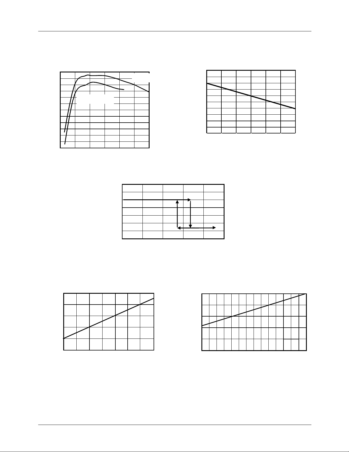
V
Typical Operating Characteristics
(V
= 5V, V
CCA
88
86
84
82
80
78
76
Efficiency (%)
74
72
70
68
66
64
0 3 6 9 12 15 18
= 12V, and T
CCP
V
Efficiency vs. Output Current
CPU
V
= 1.550V
OUT
Output Current (A)
= +25°C using circuits in Figure 1, unless otherwise noted.)
A
Droop, V
2.04
V
= 2.000
OUT
2.03
2.02
2.01
2.00
1.99
(V)
1.98
OUT
V
1.97
1.96
1.95
1.94
0 3 6 9 12 15 18
= 2.0V, RD = 8K Ω
CPU
Output Current (A)
6
CPU Output Voltage vs. Output Current
3.5
3.0
2.5
2.0
(V)
OUT
1.5
Output Programming, VID4 = 0
2.1
1.9
1.7
(V)
1.5
CPU
V
1.3
V
1.0
0.5
0
0 5 10 15 20 25
Output Current (A)
3.5
3.0
2.5
(V)
2.0
CPU
V
1.5
Output Programming, VID4 = 1
1.1
1.30 1.40 1.50 1.60 1.70 1.80 1.90 2.00
DAC Setpoint
1.0
2.1 2.2 2.3 2.4 2.5 2.6 2.7 2.8 2.9 3.0 3.1 3.2. 3.3 3.4 3.5
DAC Setpoint
REV. 1.0.0 6/30/00
 Loading...