

Fairchild Semiconductor RC5054AM Datasheet
Alpha is a trademark of Digital Equipment Corporation. Pentium is a registered trademark of Intel Corporation. PowerPC is a trademark of IBM
Corporation.
www.fairchildsemi.com
Rev. 1.0.2
Features
• Drives Two N-Channel MOSFETs
• Operates from +5V Power Input
• Simple Single-Loop Control Design
- Voltage-Mode PWM Control
• Fast Transient Response
- High-Bandwidth Error Amplifier
- Full 0% to 100% Duty Ratio
• Excellent Output Voltage Regulation
• TTL Compatible 5 Bit Digital-to-Analog Output Voltage
Selection
- Wide Range - 1.3V
DC
to 3.5V
DC
- 0.1V Binary Steps from 2.1V
DC
to 3.5V
DC
- 0.05V Binary Steps from 1.3V
DC
to 2.1V
DC
• Power-Good Output Voltage Monitor
• Over-Voltage and Over-Current Fault Monitors
- Does Not Require Extra Current Sensing Element, Uses
MOSFET’s R
DS(ON)
• Small Converter Size
- Constant Frequency Operation
- 200kHz Free-Running Oscillator Programmable from
50kHz to 1MHz
Applications
• Power Supply for Pentium
®
, Pentium Pro, PowerPC™
and Alpha™ Microprocessors
• High-Power 5V to 3.xV DC-DC Regulators
• Low-Voltage Distributed Power Supplies
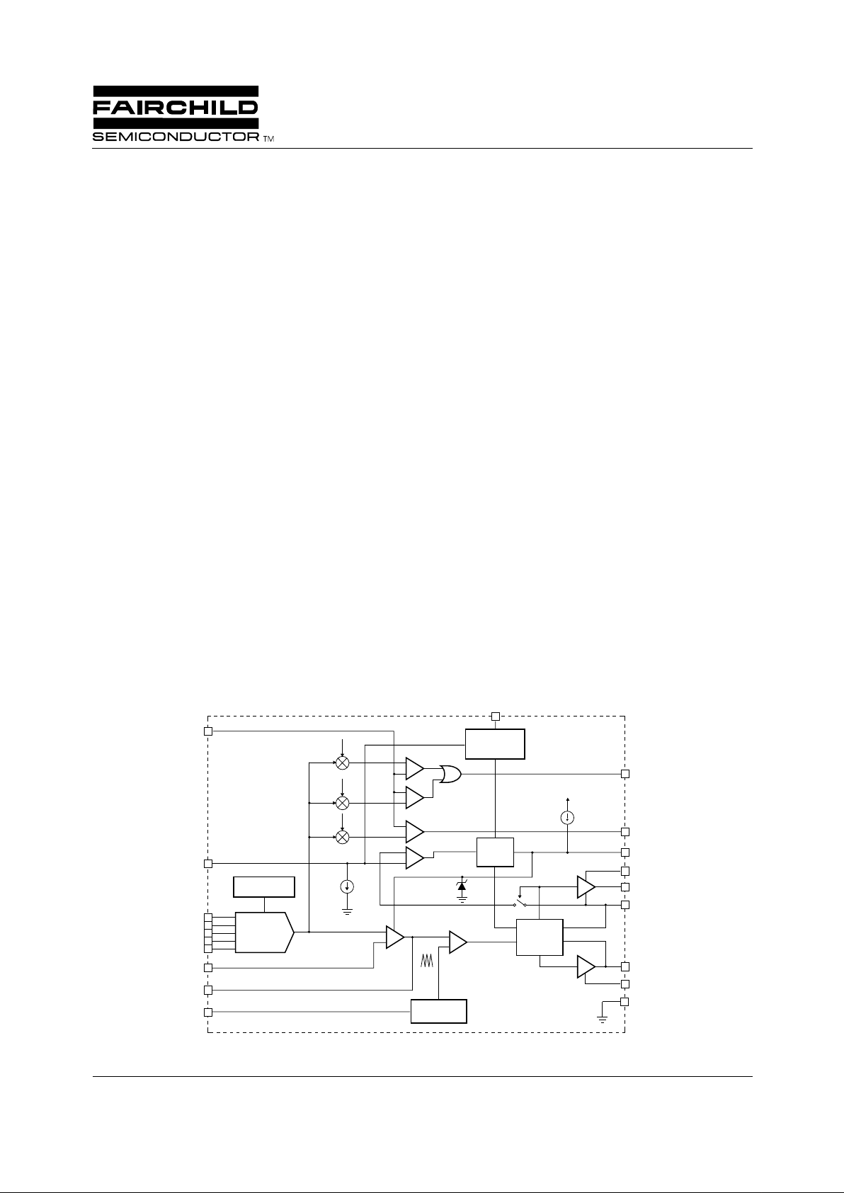
Description
The RC5054A provides complete control and protection for
a DC-DC converter optimized for high-performance microprocessor applications. It is designed to drive two N-Channel
MOSFETs in a synchronous-rectified buck topology. The
RC5054A integrates all of the control, output adjustment,
monitoring and protection functions into a single package.
The output voltage of the converter is easily adjusted and
precisely regulated. The RC5054A includes a 5-input digitalto-analog converter (DAC) that adjusts the output voltage
from 2.1V
DC
to 3.5V
DC
in 0.1V increments and from
1.3V
DC
to 2.1V
DC
in 0.05V steps.
The RC5054A provides simple, single feedback loop, volt-
RC5054A
Programmable Synchronous DC-DC Converter
Controller for Low Voltage Microprocessors
Block Diagram
D/A
CONVERTER
(DAC)
OSCILLATOR
SOFT-
START
REFERENCE
POWER-ON
RESET (POR)
115%
110%
90%
INHIBIT
PWM
COMPARATOR
ERROR
AMP
VCC
PGOOD
SS
PWM
OVP
RT
GND
VSEN
OCSET
VID0
VID1
VID2
VID3
FB
COMP
DACOUT
OVER-
VOLTAGE
OVER-
CURRENT
GATE
CONTROL
LOGIC
BOOT
UGATE
PHASE
200µA
10µA
4V
+
-
+
-
+
-
+
-
+
-
+
-
VID4
LGATE
PGND
RC5054A PRODUCT SPECIFICATION
2
age-mode control with fast transient response. It includes a
200KHz free-running triangle-wave oscillator that is adjustable from 50KHz to 1MHz. The error amplifier features a
15MHz gain-bandwidth product and 6V/ µ s slew rate which
enables high converter bandwidth for fast transient performance. The resulting PWM duty ratio ranges from 0% to
100%.
The RC5054A monitors the output voltage with a window
comparator that tracks the DAC output and issues a Power
Good signal when the output is within ± 10%. The RC5054A
protects against over-current conditions by inhibiting PWM
operation. Built-in over-voltage protection triggers an external SCR to crowbar the input supply. The RC5054A monitors the current by using the R
DS(ON)
of the upper MOSFET
which eliminates the need for a current sensing resistor.
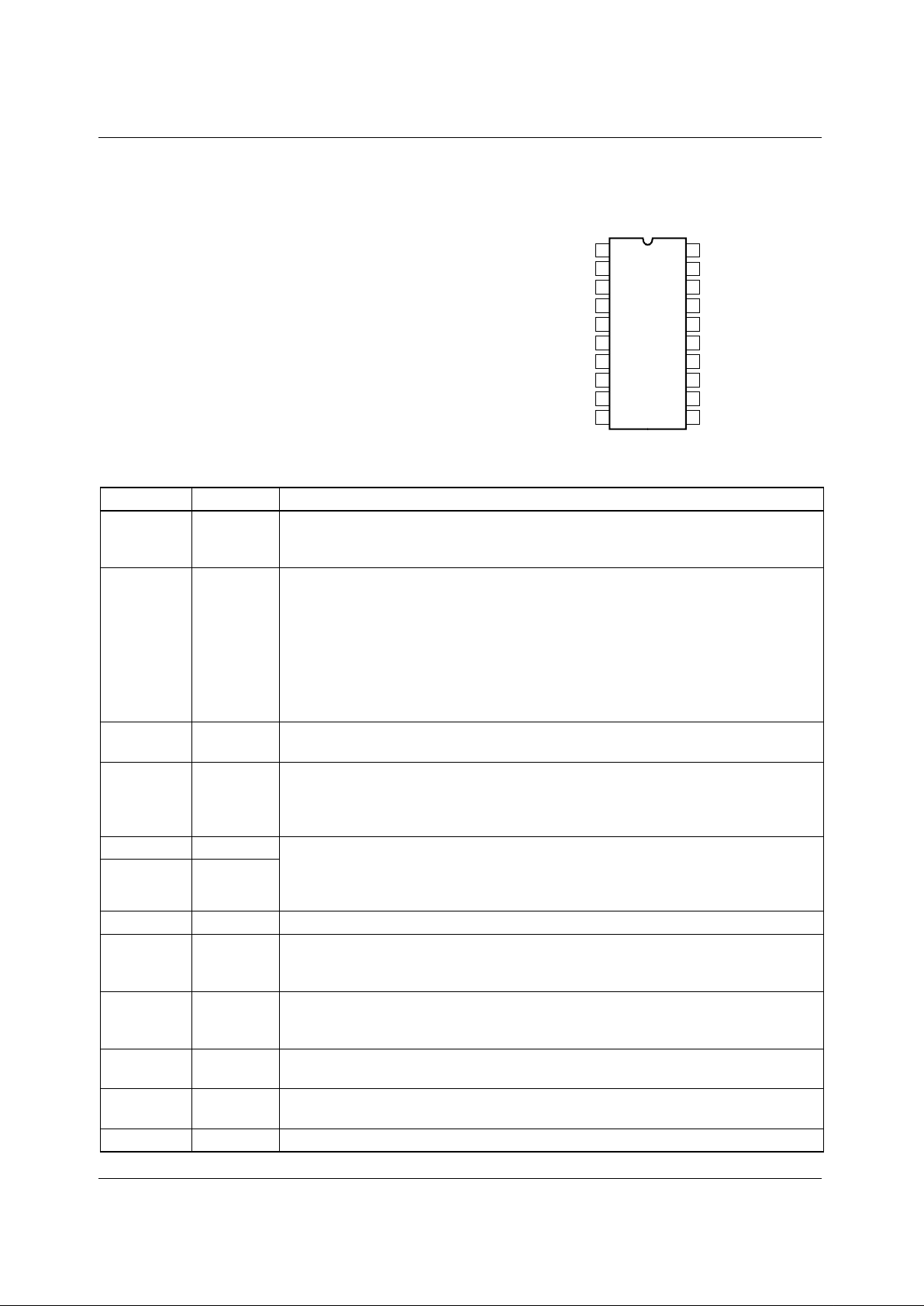
Pin Assignments
VSEN
OCSET
SS
VID0
VID1
VID2
VID4
VID3
COMP
FB
RT
VCC
LGATE
PGND
OVP
BOOT
UGATE
PHASE
PGOOD
GND
RC5054
(SOIC)
TOP VIEW
11
12
13
14
15
16
17
18
20
19
10
9
8
7
6
5
4
3
2
1
Pin Definitions
Pin Number Pin Names Pin Function Description
1 VSEN This pin is connected to the converter’s output voltage. The PGOOD and OVP
comparator circuits use this signal to report output voltage status and for overvoltage
protection.
2 OCSET Connect a resistor (R
OCSET
) from this pin to the drain of the upper MOSFET.
R
OCSET
, an internal 200 µ A current source (I
OCS
), and the upper MOSFET on-
resistance (R
DS(ON)
) set the converter over-current (OC) trip point according to the
following equation:
An over-current trip cycles the soft-start function.
3 SS Connect a capacitor from this pin to ground. This capacitor, along with an internal
10 µ A current source, sets the soft-start interval of the converter.
4-8 VID0-VID4 VID0-4 are the input pins to the 5-bit DAC. The states of these five pins program the
internal voltage reference (DACOUT). The level of DACOUT sets the converter
output voltage. It also sets the PGOOD and OVP thresholds. Table 1 specifies
DACOUT for the 32 combinations of DAC inputs.
9 COMP COMP and FB are the available external pins of the error amplifier. The FB pin is the
inverting input of the error amplifier and the COMP pin is the error amplifier output.
These pins are used to compensate the voltage-control feedback loop of the
converter.
10 FB
11 GND Signal ground for the IC. All voltage levels are measured with respect to this pin.
12 PGOOD PGOOD is an open collector output used to indicate the status of the converter
output voltage. This pin is pulled low when the converter output is not within ± 10% of
the DACOUT reference voltage.
13 PHASE Connect the PHASE pin to the upper MOSFET source. This pin is used to monitor
the voltage drop across the MOSFET for over-current protection. This pin also
provides the return path for the upper gate drive.
14 UGA TE Connect UGATE to the upper MOSFET gate. This pin provides the gate drive for the
upper MOSFET.
15 BOOT This pin provides bias voltage to the upper MOSFET driver. A bootstrap circuit may
be used to create a BOOT voltage suitable to drive a standard N-Channel MOSFET.
16 PGND This is the power ground connection. Tie the lower MOSFET source to this pin.
I
PEAK
I
OCSROCSET
•
R
DS ON()
----------------------------------------=

PRODUCT SPECIFICATION RC5054A
3
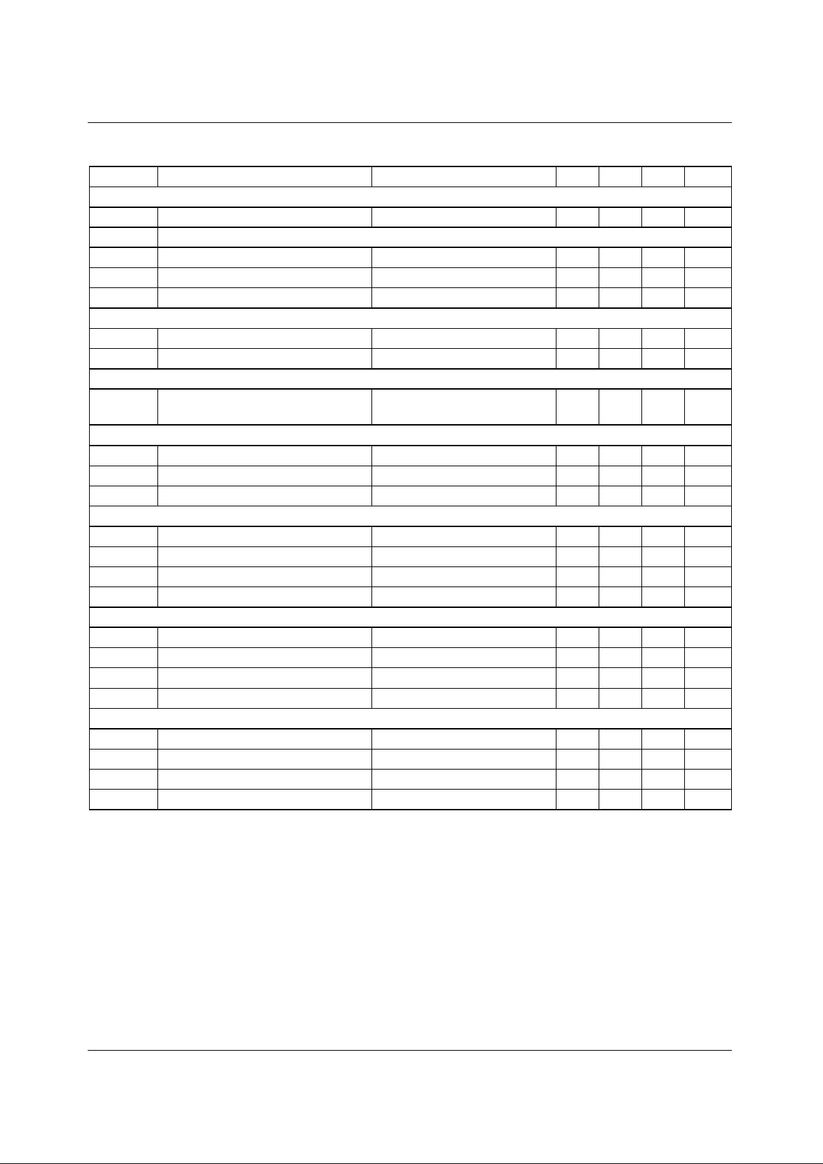
Absolute Maximum Ratings
Recommended Operating Conditions
Thermal Characteristics
NOTE:
1.
θ
JA
is measured with the component mounted on an evaluation PC board in free air.
17 LGATE Connect LGATE to the lower MOSFET gate. This pin provides the gate drive for the
lower MOSFET.
18 VCC Provide a 12V bias supply for the chip to this pin.
19 OVP The OVP pin can be used to drive an external SCR in the event of an overvoltage
condition.
20 RT This pin provides oscillator switching frequency adjustment. By placing a resistor
(R
T
) from this pin to GND, the nominal 200KHz switching frequency is increased
according to the following equation:
Conversely, connecting a pull-up resistor (RT) from this pin to VCC reduces the
switching frequency according to the following equation:
Min. Max.
Power Input Voltage, V
IN
6V
Supply Voltage, V
CC
+13.5V
Boot Voltage, V
BOOT
- V
PHASE
+13.5V
V
CC
or I/O Voltage GND -0.3V V
CC
+ 0.3V
ESD Classification Class 2
Min. Max.
Supply Voltage, V
CC
+12V -10% +12V +10%
Ambient Temperature Range 0 ° C 70 ° C
Junction Temperature Range 0 ° C 125 ° C
Parameter Conditions Min. Typ. Max. Units
Thermal Resistance
1
θ
JA
SOIC Package
SOIC Package With 3in
2
of Copper
110
86
°
C/W
°
C/W
Maximum Junction Temperature Plastic Package 150
°
C
Maximum Storage Temperature Range -65 150
°
C
Maximum Lead Temperature Soldering 10s 300
°
C
Pin Definitions
(continued)
Pin Number Pin Names Pin Function Description
S
200kHz
3.5 10
6
× KHz x Kohm[]
R
T
Kohm[]
------------------------------------------------------------+= R
T
to GND(
)
FS200kHz
310
5
× KHz x Kohm[]
R
T
Kohm[]
------------------------------------------------------- -
–= R
T
to 12V()
RC5054A PRODUCT SPECIFICATION
4
Electrical Specifications
(Recommended Operating Conditions unless otherwise specified)
Symbol Parameter Test Conditions Min. Typ. Max. Units
VCC Supply Current
I
CC
Nominal Supply UGATE and LGATE Open – 22 – mA
Power-On Reset
Rising VCC Threshold V
OCSET
= 4.5V – – 10.4 V
Falling VCC Threshold V
OCSET
= 4.5V 8.8 – – V
Rising V
OCSET
Threshold – 1.26 – V
Oscillator
Free Running Frequency RT = OPEN 185 200 215 KHz
∆
V
OSC
Ramp Amplitude RT = Open – 1.9 – V
P-P
Reference and DAC
Initial Voltage Setpoint I
LOAD
= 0.8A, V
OUT
= 2.000V
V
OUT
= 1.550V
1.980
1.534
2.000
1.550
2.020
1.566VV
Error Amplifier
DC Gain – 88 – dB
GBW Gain-Bandwidth Product – 15 – MHz
SR Slew Rate COMP = 10pF – 6 – V/ µ s
Gate Drivers
I
UGATE
Upper Gate Source V
BOOT
- V
PHASE
= 12V 350 500 – mA
I
UGATE
Upper Gate Sink V
UGATE
- V
PHASE
= 1V – 100 – mA
I
LGATE
Lower Gate Source V
CC
= 12V, V
LGATE
= 6V 300 450 – mA
I
LGATE
Lower Gate Sink V
UGATE
- V
PHASE
= 1V – 100 – mA
Protection
Over-Voltage Trip (V
SEN
/DACOUT) – 115 120 %
I
OCSET
OCSET Current Source V
OCSET
= 4.5V
DC
170 200 230 µA
I
OVP
OVP Sourcing Current V
SEN
= 5.5V, V
OVP
= 0V 60 – – mA
I
SS
Soft Start Current – 10 – µA
Power Good
Upper Threshold (V
SEN
/DACOUT) VSEN Rising 106 – 111 %
Lower Threshold (V
SEN
/DACOUT) VSEN Falling 89 – 94 %
Hysteresis (V
SEN
/DACOUT) Upper and Lower Threshold – 2 – %
V
PGOOD
PGOOD Voltage Low I
PGOOD
= -5mA – 0.5 – V
 Loading...