

Fairchild Semiconductor RC5037 Datasheet
www.fairchildsemi.com
RC5037
Adjustable Switching Regulator Controller
Features
• High power switch-mode DC-DC controller can provide
in excess of 13A
• Output voltage adjustable from 1.5V to 3.6V
• 85% efficiency
• Cumulative accuracy < 3% over line, load, and
temperature variations
• Overvoltage and short circuit protection
• Built-in soft start
Applications
• I/O and AGP power for desktop computers
• High efficiency power for ASICs
• High efficiency power for DSPs
• Adjustable step-down power supplies
Description
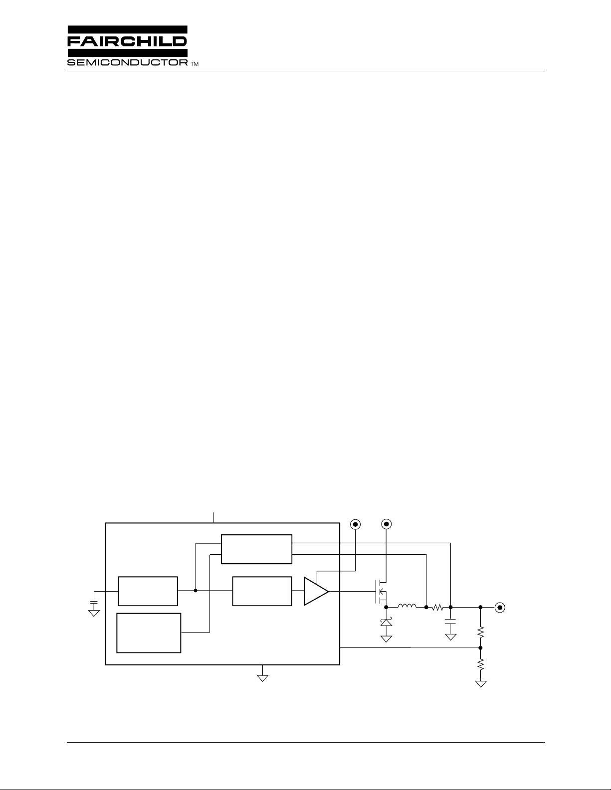
The RC5037 is a high power, switch-mode DC-DC controller
that provides efficient power for all lo w-voltage applications.
This controller has a built-in Soft Start feature which offers
system protection during power-up by reducing both inrush
current and output overshoot. When combined with the
appropriate external circuitry, the RC5037 can deliver load
currents as high as 13A at efficiencies as high as 88%. The
RC5037 can generate output voltages from 1.5V up to 3.6V
using external resistors.
The RC5037 is designed to operate in a constant on-time
control mode under all load conditions. Its accurate low TC
reference eliminates the need for precision external components in order to achieve the tight tolerance voltage regulation required by many applications. Short circuit current
protection is provided through the use of a current sense
resistor, while overvoltage protection is provided internally.
Block Diagram
RC5037
Oscillator
1
1.5V
Reference
2
Feedback Control
Digital Logic
+12V5V +5V
4
3
8
7
Vout
5
6
REV. 1.0.1
.
.
RC5037 PRODUCT SPECIFICATION
Pin Assignments
Pin Descriptions
Pin
Name
CEXT 1
VCCA 2
IFBH 3
IFBL 4
VFB 5
GNDP 6
DRV 7
VCCP 8
Pin
Number Pin Function Description
External capacitor. A 180pF capacitor is connected to this pin as part of the constant on-
time pulse width circuit. Careful layout of this pin is critical to system performance. See
Applications Information for details.
Analog V
system 5V supply and decouple to ground with 0.1µF ceramic capacitor.
High side current feedback. Pins 3 and 4 are used as the inputs for the current feedback
control loop and as the short circuit current sense points. Careful layout of the traces from
these pins to the current sense resistor is critical for optimal performance of the short circuit
protection scheme. See Applications Information for details.
Low side current feedback. See Applications Information for details.
Voltage feedback. Using two external resistors, this pin sets the output voltage level for the
switching regulator.
Power Ground. Connect to a low impedance ground. See Application Information for
details.
MOSFET driver output. Connect this pin to the gate of the N-channel MOSFET Q1 as
shown in Figure 12. The trace from this pin to the MOSFET gate should be kept as short as
possible (less than 0.5"). See Applications Information for details.
Power V
filter shown in Figure 12. See Applications Information for details.
CEXT
VCCA
IFBH
IFBL VFB
Power supply for regulator control circuitry and voltage reference. Connect to
cc
Power supply for DRV output driver. Connect to system 12V supply with R-C
cc
1
2
3
45
RC5037
VCCP
8
DRV
7
GNDP
6
Absolute Maximum Ratings
Supply V oltages, VCCA 7V
Supply V oltages, VCCP 13V
Junction Temperature, T
Storage Temperature, T
J
S
+150°C
-65 to +150°C
Lead Soldering Temperature, 10 seconds 300°C
Thermal Resistance Junction-to-Ambient, Θ
Note:
1. Functional operation under any of these conditions is not implied. Performance is guaranteed only if Operating Conditions
are not exceeded.
JA
163°C/W
Operating Conditions
Parameter Conditions Min. Typ. Max. Units
Switching Regulator Supply, VCCA 4.75 5 5.25 V
Ambient Operating Temperature, T
A
Gate Drive Supply, VCCP 9.5 12 12.6 V
2
070°C
•
•
•
•
•
PRODUCT SPECIFICATION RC5037
Electrical Characteristics
(VCCA = 5V, VCCP = 12V, T
The • denotes specifications which apply over the full ambient operating temperature range.
Parameter Conditions Min. Typ. Max. Units
Output Voltage 1.5 3.6 V
Output Temperature Drift T
Line Regulation VCCA = 4.75 to 5.25V, I
Load Regulation I
V
PSRR VCCA = 4.75 to 5.25V 60 dB
OUT
Output Ripple, peak-peak 20MHz BW, I
Total DC Accuracy
1
Efficiency I
Output Driver Current Open Loop
Short Circuit Threshold Voltage
On Time Pulse Width
VCCA Supply Current Independent of load
VCCP Supply Current I
= 25
°
A
C using circuit of Figure 1, unless otherwise noted)
= 0˚C–70˚C 40 ppm/˚C
A
= 13A 3 5 mV
LOAD
= 0 to 5A or 5A to 13A 30 43 mV
LOAD
= 13A 15 mV
LOAD
±55 ±100 mV
= 5A 80 85 %
LOAD
0.5 A
70 90 100 mV
2
C
= 180pF 3.5 µs
EXT
515mA
LOAD
= 13A
20 25 mA
Notes:
1. Total DC accuracy includes setpoint accuracy, temperature drift, line and load regulation.
2. The on-time pulse width of the oscillator is set via external capacitor C
EXT
.
3

RC5037 PRODUCT SPECIFICATION
Typical Operating Characteristics
(VCCA = 5V, and T
= +25
A
°
C using circuit in Figure 1, unless otherwise noted)
95
94
93
92
91
90
89
88
Efficiency (%)
87
86
85
12 3 4 5
Efficiency vs. Output Current
678910
Output Current
Output Voltage vs. Temperature, I
+0.50
+0.25
Nom.
-0.25
Output Voltage (%)
-0.50
0255075
Output Voltage vs. Load
+1.5
+1.0
+0.5
(%)
Nom
OUT
V
-0.5
-1.0
-1.5
02468
Output Current (A)
= 10A
OUT
100 125
10
Transient Response, 0.5 to 5.5A
(50mV/div)
OUT
(2A/div) V
SW
I
Time (100µs/division)
Output Ripple, I
(10mV/division)
OUT
V
= 10A)
OUT
Time (2µs/division)
4
 Loading...