

Fairchild Semiconductor RC1585 Datasheet
www.fairchildsemi.com
RC1585
5A Adjustable/Fixed Low Dropout Linear Regulator
Features
• Fast transient response
• Low dropout voltage at up to 5A
• Load regulation: 0.05% typical
• Trimmed current limit
• On-chip thermal limiting
• Standard TO-220, TO-263, TO-263 center cut and TO-252
packages
Applications
• Pentium® class GTL+ bus supply
• Low voltage logic supply
• Post regulator for switching supply
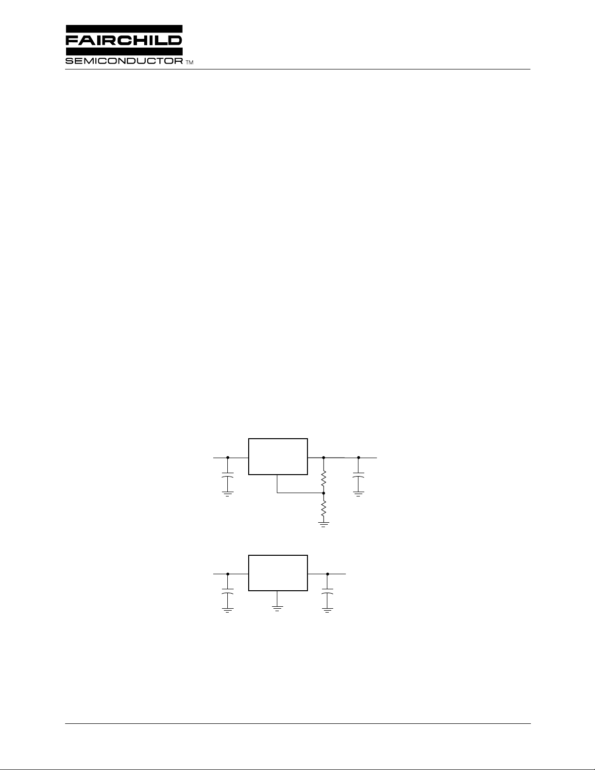
Typical Applications
RC1585
V
IN
= 3.3V
10µF
V
IN
+
ADJ
Description
The RC1585 and RC1585-1.5 are low dropout three-terminal
regulators with 5A output current capability. These devices
have been optimized for low voltage applications including
bus termination, where transient response and mini-
V
TT
mum input voltage are critical. The RC1585 is ideal for low
voltage microprocessor applications requiring a regulated
output from 1.5V to 3.6V with an input supply of 5V or less.
The RC1585-1.5 offers fixed 1.5V with 5A current capabilities for GTL+ bus V
Current limit is trimmed to ensure specified output current
and controlled short-circuit current. On-chip thermal limiting provides protection against any combination of overload
and ambient temperature that would create excessive junction temperatures.
The RC1585 series regulators are available in the industrystandard TO-220, TO-263, TO-263 center cut and TO-252
power packages.
V
OUT
124Ω
+
22µF
termination.
TT
1.5V at 5A
24.9Ω
RC1585-1.5
= 3.3V
V
IN
10µF
Pentium is a registered trademark of Intel Corporation. REV. 1.1.4 10/8/02
V
+
V
IN
OUT
GND
+
22µF
1.5V at 5A
65-1585-01a
RC1585 PRODUCT SPECIFICATION
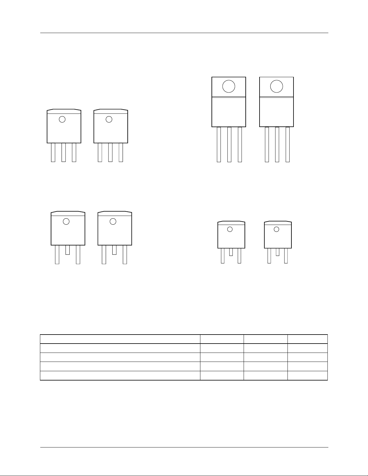
Pin Assignments
RC1585T-1.5RC1585T
FRONT VIEW
FRONT VIEW
RC1585MRC1585M-1.5
FRONT VIEW
FRONT VIEW
12 3
12 3
GND
FRONT VIEW
IN
3-Lead Plastic TO-263
θJC = 3°C/W*
12 3
GND
3-Lead Plastic TO-263 Center Cut
IN
θJC = 3°C/W*
12 3
IN
RC1585MCRC1585MC-1.5
FRONT VIEW
12 3
ADJ
IN
Tab is Out.
ADJ
OUT
INADJ
3-Lead Plastic TO-220
θJC = 3°C/W
FRONT VIEW
12 3
GND
IN
3-Lead Plastic TO-252
θJC = 3°C/W*
12 3
GND OUTOUT OUT
RC1585DRC1585D-1.5
FRONT VIEW
12 3
ADJ
IN
Tab is Out.
IN
* θJA can vary from 20°C/W to >40°C/W with various mounting techniques.
65-1585-02
Absolute Maximum Ratings
Parameter Min. Max. Unit
V
IN
Operating Junction Temperature Range 0 125 °C
Storage Temperature Range -65 150 °C
Lead Temperature (Soldering, 10 sec.) 300 °C
2 REV. 1.1.4 10/8/02
7V
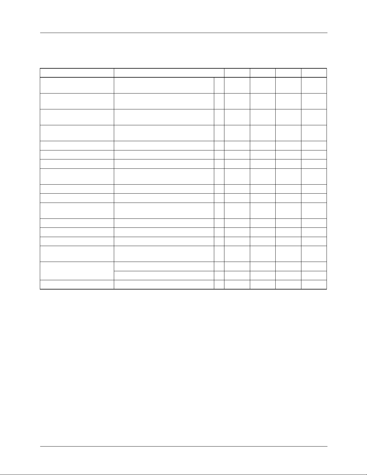
PRODUCT SPECIFICATION RC1585
Electrical Characteristics
Tj = 25°C unless otherwise specified.
The • denotes specifications which apply over the specified operating temperature range.
Parameter Conditions Min. Typ. Max Units
Reference Voltage
Output Voltage
Line Regulation
Load Regulation
3
4
1, 2
1, 2, 3
Dropout Voltage ∆V
Current Limit (VIN – V
Adjust Pin Current
3
Adjust Pin Current Change31.5V ≤ (VIN – V
Minimum Load Current 1.5V ≤ (VIN – V
Quiescent Current VIN = 5V • 413mA
Ripple Rejection f = 120Hz, C
Thermal Regulation TA = 25°C, 30ms pulse 0.004 0.02 %/W
Temperature Stability • 0.5 %
Long-Term Stability TA = 125°C, 1000 hrs. 0.03 1.0 %
RMS Output Noise
(% of V
OUT
)
Thermal Resistance,
Junction to Case
Thermal Shutdown 150 °C
Notes:
1. See thermal regulation specifications for changes in output voltage due to heating effects. Load and line regulation are
measured at a constant junction temperature by low duty cycle pulse testing.
2. Line and load regulation are guaranteed up to the maximum power dissipation (18W). Power dissipation is determined by
input/output differential and the output currrent. Guaranteed maximum output power will not be available over the full input/
output voltage range.
3. RC1585 only.
4. RC1585-1.5 only.
1.5V ≤ (VIN – V
10mA ≤ I
OUT
3V ≤ VIN ≤ 7V
10mA ≤ I
(V
I
OUT
(VIN – V
10mA ≤ I
OUT
+ 1.5V) ≤ VIN ≤ 7V,
OUT
= 10mA
) = 3V,
OUT
OUT
= 1%, I
REF
) = 2V • 5.1 5.5 A
OUT
OUT
≤ 5A
) ≤ 5.75V,
• 1.225
(-2%)
1.250 1.275
(+2%)
• 1.47 1.5 1.53 V
≤ 5A
• 0.005 0.2 %
• 0.05 0.5 %
≤ 5A
= 5A • 1.150 1.300 V
OUT
V
• 35 120 µA
10mA ≤ I
(VIN – V
OUT
OUT
) ≤ 5.75V,
OUT
≤ 5A
) ≤ 5.75V • 10 mA
OUT
= 22µF Tantalum,
OUT
) = 3V, I
OUT
= 5A
• 0.2 5 µA
60 72 dB
TA = 25°C, 10Hz ≤ f ≤ 10kHz 0.003 %
TO-220 3 °C/W
TO-263, TO-252 3 °C/W
REV. 1.1.4 10/8/02 3
RC1585 PRODUCT SPECIFICATION
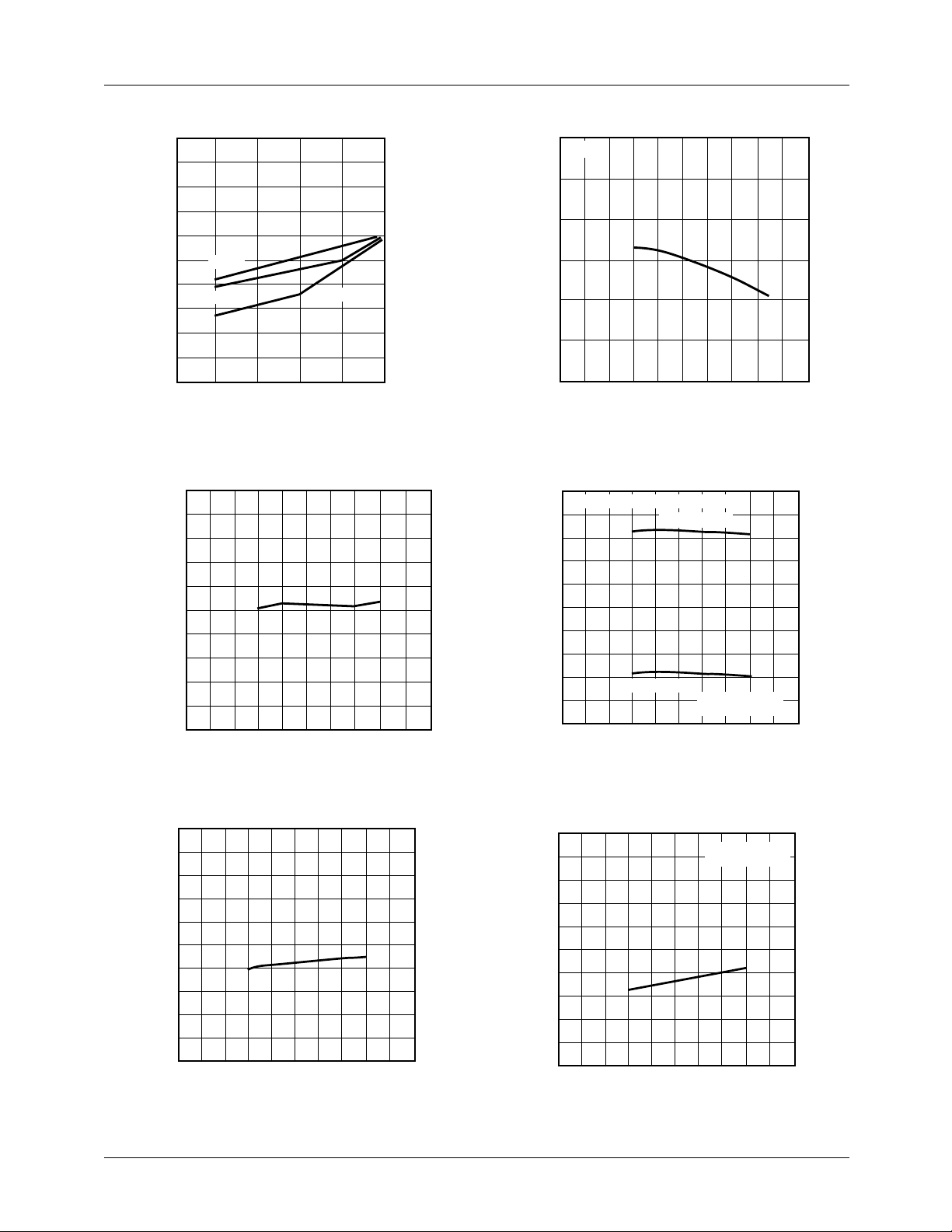
Typical Performance Characteristics
1.5
1.4
1.3
1.2
1.1
1.0
0.9
0.8
DROPOUT VOLTAGE (V)
0.7
T=0°C
T=25°C
T=125°C
0.6
0.5
123
450
65-1585-03
OUTPUT CURRENT (A)
Figure 1. Dropout Voltage vs. Output Current Figure 2. Load Regulation vs. Temperature
0.10
∆I = 5A
0.05
0
-0.05
-0.10
-0.15
OUTPUT VOLTAGE DEVIATION (%)
-0.20
-75 -50 -25 0 25 50 75 100 125 150 175
JUNCTION TEMPERATURE (°C)
65-1585-04
1.275
1.270
1.265
1.260
1.255
1.250
1.245
1.240
REFERENCE VOLTAGE (V)
1.235
1.230
1.225
-75 -50 -25 0 25 50 75 100 125 150 175
65-1585-05
JUNCTION TEMPERATURE (°C)
3.70
V
SET WITH 1% RESISTORS
OUT
3.65
3.60
3.55
3.50
3.45
3.40
3.35
REFERENCE VOLTAGE (V)
3.30
3.25
3.20
-75 -50 -25 0 25 50 75 100 125 150 175
JUNCTION TEMPERATURE (°C)
V
OUT
V
OUT
= 3.3V
= 3.6V
1
Note:
1. RC1585 Only
1
65-1585-06
Figure 3. Reference Voltage vs. Temperature Figure 4. Output Voltage vs. Temperature
5
4
3
2
1
MINIMUM LOAD CURRENT (mA)
0
-75 -50 -25 0 25 50 75 100 125 150 175
JUNCTION TEMPERATURE (°C)
65-1585-07
100
90
80
70
60
50
40
30
20
ADJUST PIN CURRENT (µA)
10
0
-75 -50 -25 0 25 50 75 100 125 150 175
JUNCTION TEMPERATURE (°C)
Note:
1. RC1585 Only
65-1585-08
Figure 5. Minimum Load Current vs. Temperature Figure 6. Adjust Pin Current vs. Temperature
4 REV. 1.1.4 10/8/02
 Loading...