Fairchild Semiconductor QVE00120 Datasheet

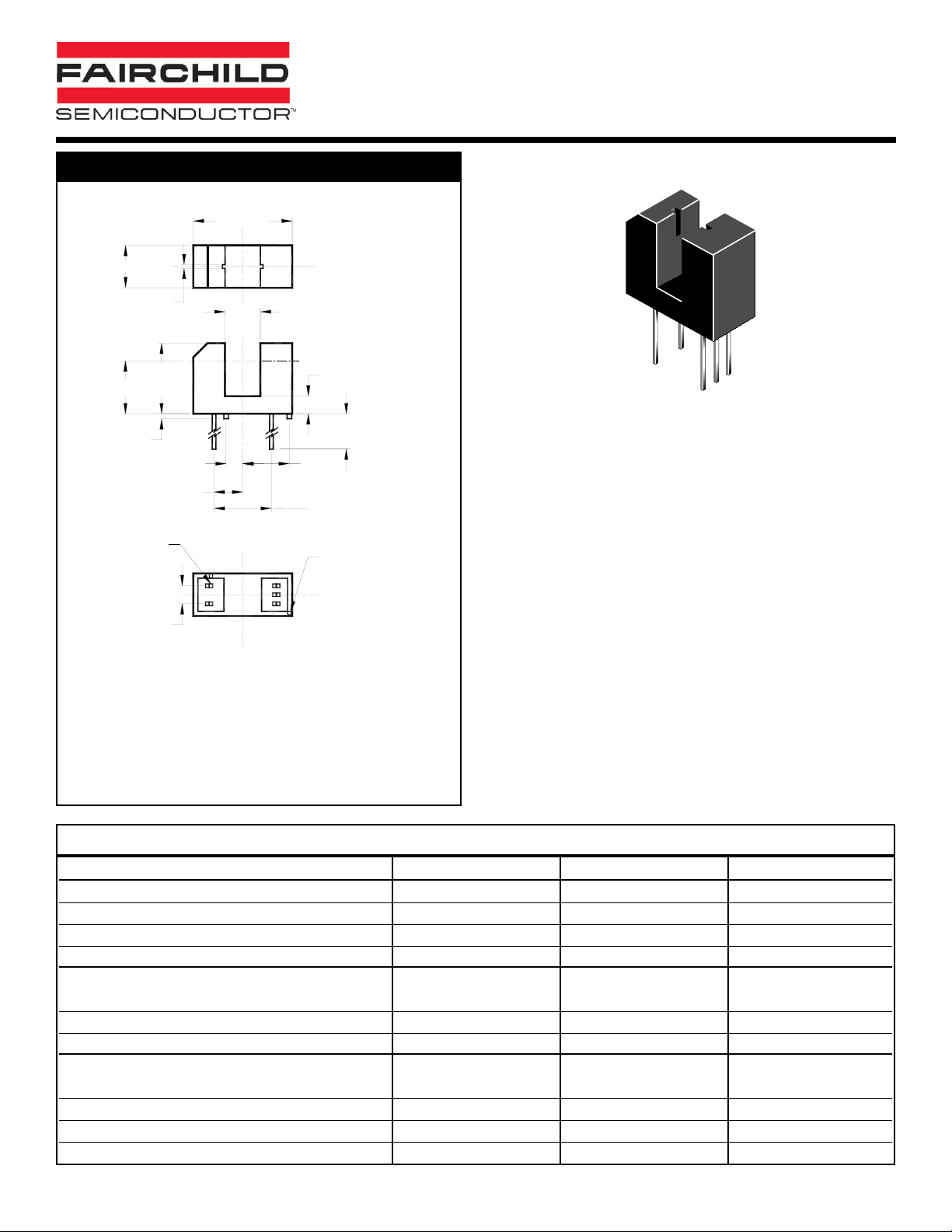
PACKAGE DIMENSIONS
C
L
+
E
D
+
PIN #1 (ANODE)
PIN #2 (CATHODE)
1
2
5
3
C.L.
OPTICAL
C
L
L
C
C
L
OPTICAL
C.L.
PIN #3 (VCC)
PIN #4 (VOUT)
PIN #5 (GND)
4
.260
(6.60)
PINS
.020 (.51) (4x)
SQ. (TYP)
KNOB
Ø.026 (.66)
(2X)
.320 (8.128)
(TYP)
.092 (2.35)
.160 (4.064)
(2X TYP)
.197
(5.00)
.100 (2.50)
.197 (5.00) MIN
(4X)
.027 (.70)
(2X)
.295 (7.50)
.394 (10.00)
(2X)
.020 (.50)
.551 (14.00)
.236 (6.00)
.100 (2.54) (2X)
(TYP)
NOTES:
1. Dimensions for all drawings are in inches (millimeters).
2. Tolerance of ± .010 (.25) on all non-nominal dimensions
unless otherwise specified.
NOTES (Applies to Max Ratings and Characteristics Tables.)
1. Derate power dissipation linearly 1.67 mW/°C above 25°C.
2. Derate power dissipation linearly 2.50 mW/°C above 25°C.
3. RMA flux is recommended.
4. Methanol or isopropyl alcohols are recommended as
cleaning agents.
5. Soldering iron
1/16” (1.6mm) from housing.
6. As long as leads are not under any stress or spring tension.
FEATURES
• No contact switching
• 5.0 mm wide slot
• 0.5 mm aperture width
• Opaque black plastic housing
• Output configuration: Buffer open-collector
• TTL/CMOS compatible output
• Locating knobs on housing base for accurate mounting
1 of 5 100029B
Parameter Symbol Rating Units
Operating Temperature T
OPR
-40 to +85 °C
Storage Temperature T
STG
-40 to +85 °C
Lead Temperature (Solder Iron)
(3,4,5,6)
T
SOL-I
240 for 5 sec °C
Lead Temperature (Solder Flow)
(3,4,5,6)
T
SOL-F
260 for 10 sec °C
EMITTER
Continuous Forward Current I
F
50 mA
Reverse Voltage V
R
5V
Power Dissipation
(1)
P
D
100 mW
SENSOR
Output Current I
O
50 mA
Supply Voltage V
CC
16 V
Output Voltage V
O
30 V
Power Dissipation
(2)
P
D
150 mW
ABSOLUTE MAXIMUM RATINGS
(TA= 25°C unless otherwise specified)
QVE00120
OPTOLOGIC®OPTICAL
INTERRUPTER SWITCH

2 of 5 100029B
QVE00120
OPTOLOGIC®OPTICAL
INTERRUPTER SWITCH
PARAMETER TEST CONDITIONS SYMBOL MIN. TYP. MAX. UNITS
Operating Supply Voltage V
CC
4.5 16 V
INPUT DIODE
Forward Voltage I
F
= 20 mA V
F
— 1.7 V
Reverse Leakage Current VR= 5 V I
R
—10
µ
A
COUPLED
Operating Supply Current I
F
= 15 mA or 0 mA, V
CC
= 16 V I
CC
—5mA
Low Level Output Voltage IF= 15 mA, V
CC
= 5 V, RL= 360 ! V
OL
— 0.4 V
High Level Output Current IF= 0 mA, V
CC
= 5 V, VOH= 30 V I
OH
— 100
µ
A
Turn on Threshold Current V
CC
= 5 V, RL= 360 ! IF(+) — 15 mA
Turn off Threshold Current V
CC
= 5 V, RL= 360 ! IF(-) 0.50 — mA
Hysteresis Ratio IF(+) / IF(-) 1.2
Propagation Delay V
CC
= 5 V, RL= 360 ! t
PLH, tPHL
5
µ
s
Output Rise and Fall Time V
CC
= 5 V, RL= 360 ! t
r, tf
70 ns
ELECTRICAL / OPTICAL CHARACTERISTICS
(TA =25°C)
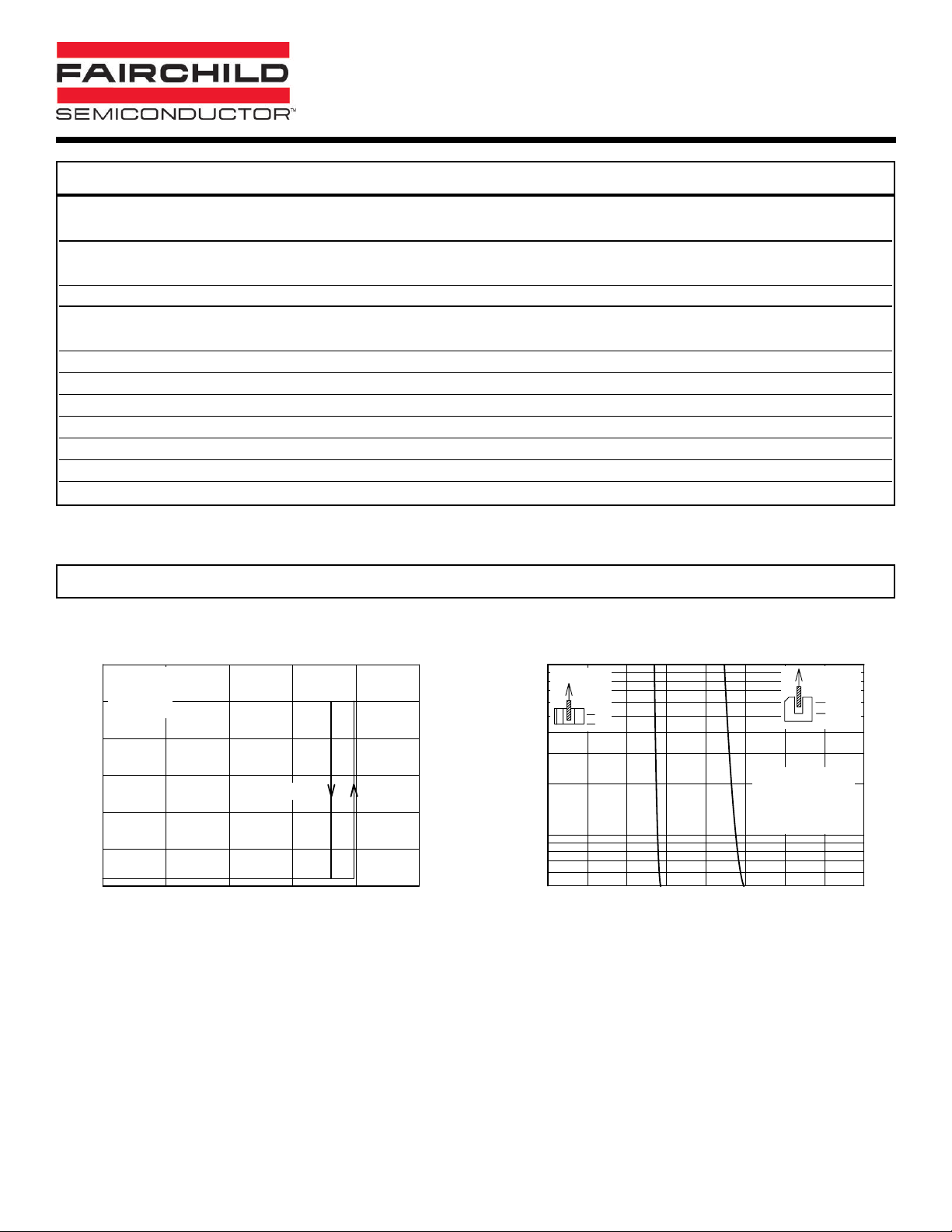
TYPICAL PERFORMANCE CURVES
Fig. 1 Output Voltage vs. Input Current
6
VCC = 5 V
RL = 270 !
5
= 25˚C
T
A
4
3
- Output Voltage (V)
2
O
V
1
0
012345
IF - Input Current (mA)
I
F (OFF)
V
OL
V
OH
I
F (ON)
Fig. 2 Normalized Threshold Current vs. Shield Distance
10
Black Shield
+
d
D
E
+
0
- Normalized Threshold Current
1
F (ON)
I
012345678
d - Distance (mm)
Black Shield
d
0
Normalized to:
= 5 V
V
CC
I
= 20 mA Pulsed
F
Pulse Width = 100 µs
Duty Cycle = 0.1%
 Loading...