

Fairchild Semiconductor QSE133 Datasheet
PLASTIC SILICON
INFRARED PHOTOTRANSISTOR
QSE133
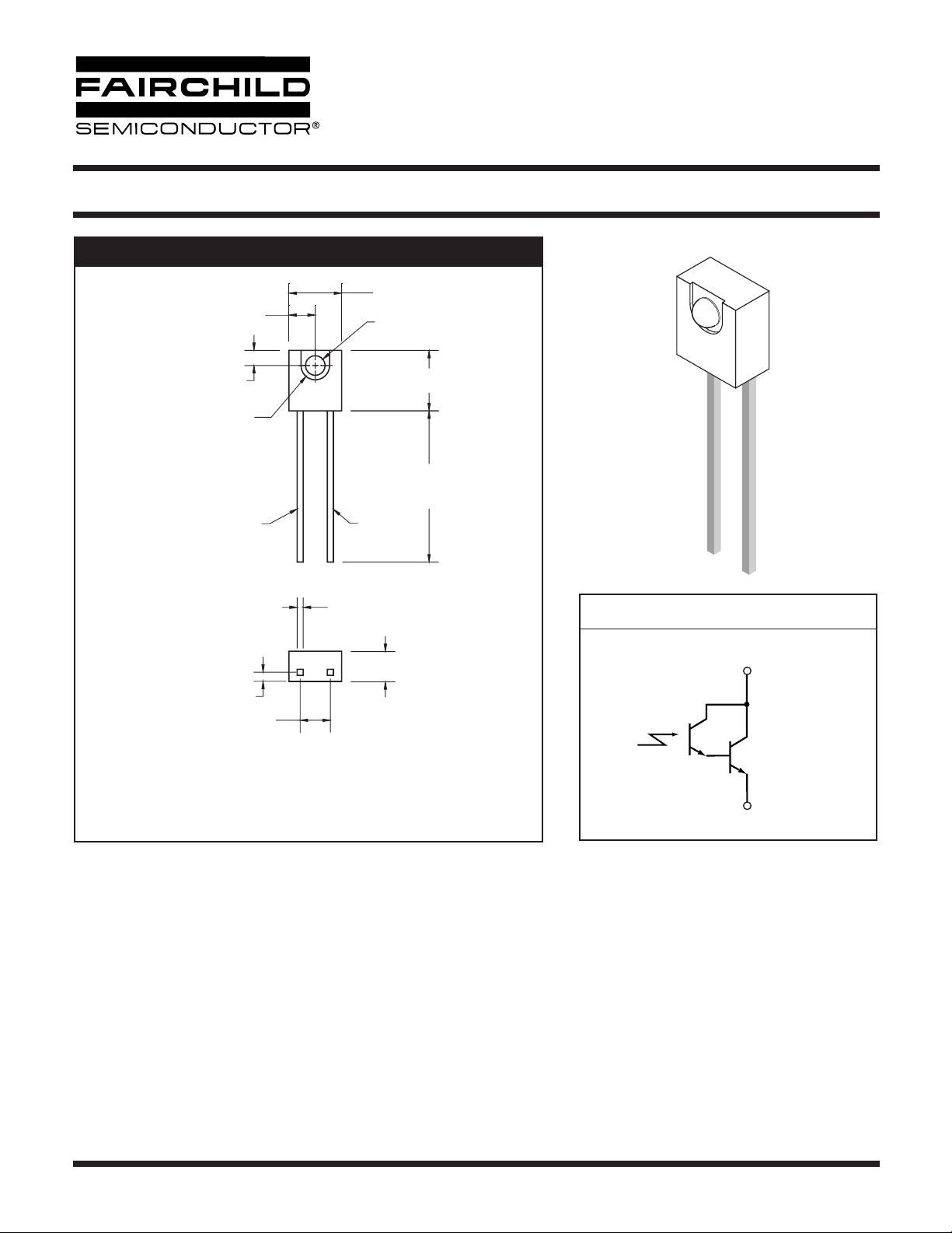
PACKAGE DIMENSIONS
0.175 (4.44)
0.087 (2.22)
Ø 0.095 (2.41)
Ø 0.065 (1.65)
0.200 (5.08)0.050 (1.27)
0.500 (12.70)
MIN
EMITTER
0.030 (0.76)
0.100 (2.54)
NOM
NOTES:
1. Dimensions for all drawings are in inches (mm).
2. Tolerance of ± .010 (.25) on all non-nominal dimensions unless
otherwise specified.
COLLECTOR
0.020 (0.51) SQ.
(2X)
0.100 (2.54)
SCHEMATIC
COLLECTOR
EMITTER
DESCRIPTION
The QSE133 is a silicon photodarlington encapsulated in a wide angle, infrared transparent, black plastic sidelooker package.
FEATURES
• NPN silicon phototransistor
• Package type: Sidelooker
• Medium wide reception angle, 50°
• Package material and color: black epoxy
• Matched emitter: QEE113
• Daylight filter
• High sensitivity
© 2002 Fairchild Semiconductor Corporation
Page 1 of 4
5/1/02
Θ
PLASTIC SILICON
INFRARED PHOTOTRANSISTOR
QSE133
ABSOLUTE MAXIMUM RATINGS
(T
= 25°C unless otherwise specified)
A
Parameter Symbol Rating Unit
Operating Temperature
Storage Temperature
Soldering Temperature (Iron)
Soldering Temperature (Flow)
Collector Emitter Voltage
Emitter Collector Voltage
Power Dissipation
(1)
(2,3,4)
(2,3)
T
T
T
SOL-I
T
SOL-F
V
V
OPR
STG
CE
EC
P
D
-40 to +100 °C
-40 to +100 °C
240 for 5 sec °C
260 for 10 sec °C
30 V
5V
100 mW
NOTES:
1. Derate power dissipation linearly 1.33 mW/°C above 25°C.
2. RMA flux is recommended.
3. Methanol or isopropyl alcohols are recommended as cleaning agents.
4. Soldering iron 1/16" (1.6 mm) minimum from housing.
5. λ = 880 nm (AlGaAs).
(T
ELECTRICAL / OPTICAL CHARACTERISTICS
=25°C unless otherwise specified)
A
Parameter Test Conditions Symbol Min Typ Max Units
Peak Sensitivity
Reception Angle
Collector Emitter Dark Current
Collector-Emitter Breakdown
Emitter-Collector Breakdown
On-State Collector Current
Saturation Voltage
(5)
(5)
Rise Time
Fall Time
V
= 10 V, E
CE
I
= 1 mA BV
C
I
= 100 µA BV
E
E
= 0.25 mW/cm
e
E
= 0.5 mW/cm
e
= 0.15mA, V
I
C
R
= 100 Ω
L
= 0 I
e
2
, V
= 5 V
CE
2
, I
= 0.4 mA
C
= 5V,
CC
λ
CEO
I
C(ON)
V
CE(SAT)
PS
CEO
ECO
t
r
t
f
— 880 — nM
— ±25 — Deg.
——100 nA
30 —— V
5 —— V
9.0 ——mA
——1.0 V
— 20 — µs
— 50 — µs
© 2002 Fairchild Semiconductor Corporation
Page 2 of 4
5/1/02
 Loading...