Fairchild Semiconductor QCK5 Datasheet

Parameter Symbol Rating Units
Operating Temperature T
OPR
-40 to +100
°C
Storage Temperature T
STG
-40 to +100
°C
Soldering Temperature (Flow)
(2,3)
T
SOL-F
Preheating Stage for 60 sec 183
°C
Reflow Stage for 5 sec 230
°C
Rate of Temperature Rise 3 to 10
°C/S
EMITTER
Continuous Forward Current I
F
50 mA
Reverse Voltage V
R
5V
Power Dissipation
(1)
P
D
100 mW
SENSOR
Collector-Emitter Voltage V
CEO
30 V
Emitter-Collector Voltage V
ECO
4V
Power Dissipation
(1)
P
D
100 mW
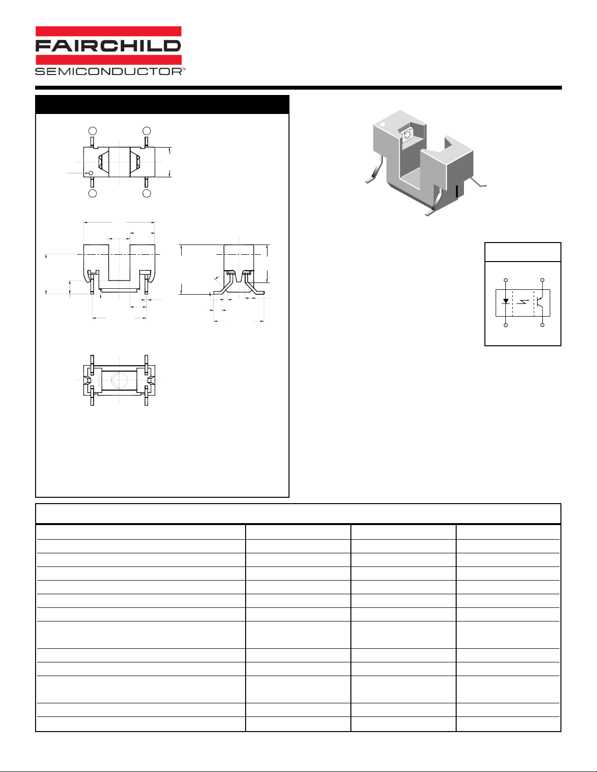
PACKAGE DIMENSIONS
L
C
0.365±0.020
(4X)
0.280
0.0283
0.060±0.020
(4X)
0.085
0.370±0.020
0.157
0.185
0.527
0.100±0.005
0.015
0.1215
0.020SQ
0.400±0.020
(4X)
(2X)
45.0°
2
0.2200
L
C
PIN 1
IDENTIFICATION
0.295±0.005
(4X)
C
L
L
C
PIN 1 CATHODE
PIN 2 ANODE
PIN 3 EMITTER
PIN 4 COLLECTOR
3
4
1
OPTICAL C
L
C
L
L
OPTICAL C OPTICAL C
L
C
L
NOTES:
1. Dimensions for all drawings are in inches.
2. Tolerance of ± .010 on all non-nominal dimensions
unless otherwise specified.
3. All leads are coplanar within .006”.
4. Housing material is electrically conductive.
NOTES (Applies to Max Ratings and Characteristics Tables.)
1. Derate power dissipation linearly 1.67 mW/°C above 25°C.
2. RMA flux is recommended.
3. Methanol or isopropyl alcohols are recommended as
cleaning agents.
1 of 5 100010F
QCK5
PHOTOTRANSISTOR OPTICAL
INTERRUPTER SWITCH
FEATURES
• No contact switching
• 4 mm wide slot
• Leads formed for surface mounting
• Housing material resistant to high
temperatures
• Daylight filter on sensor
• Transistor Output
• Tape & Reel Option: .TR (See Tape & Reel Dimensions)
SCHEMATIC
ABSOLUTE MAXIMUM RATINGS
(TA= 25°C unless otherwise specified)
2
1
3
4

PARAMETER TEST CONDITIONS SYMBOL MIN TYP MAX UNITS
EMITTER
Forward Voltage I
F
= 20 mA V
F
——1.7 V
Reverse Current VR= 5 V I
R
——100
µ
A
Peak Emission Wavelength IF= 20 mA
!
PE
— 940 — nm
SENSOR
Collector-Emitter Breakdown I
C
= 1 mA BV
CEO
30 —— V
Emitter-Collector Breakdown IE= 0.1 mA BV
ECO
5 —— V
Dark Current VCE= 10 V, IF= 0 mA I
D
——100 nA
COUPLED
Collector Current I
F
= 20 mA, VCE= 5 V I
C(ON)
2.0 —— mA
Collector Emitter IF= 20 mA, IC = 0.5 mA V
CE (SAT)
——0.4 V
Saturation Voltage
Rise Time VCE= 5 V, RL = 100 " t
r
— 8 —
µ
s
Fall Time I
C
= 5 mA t
f
— 50 —
µ
s
QCK5
PHOTOTRANSISTOR OPTICAL
INTERRUPTER SWITCH
2 of 5 100010F
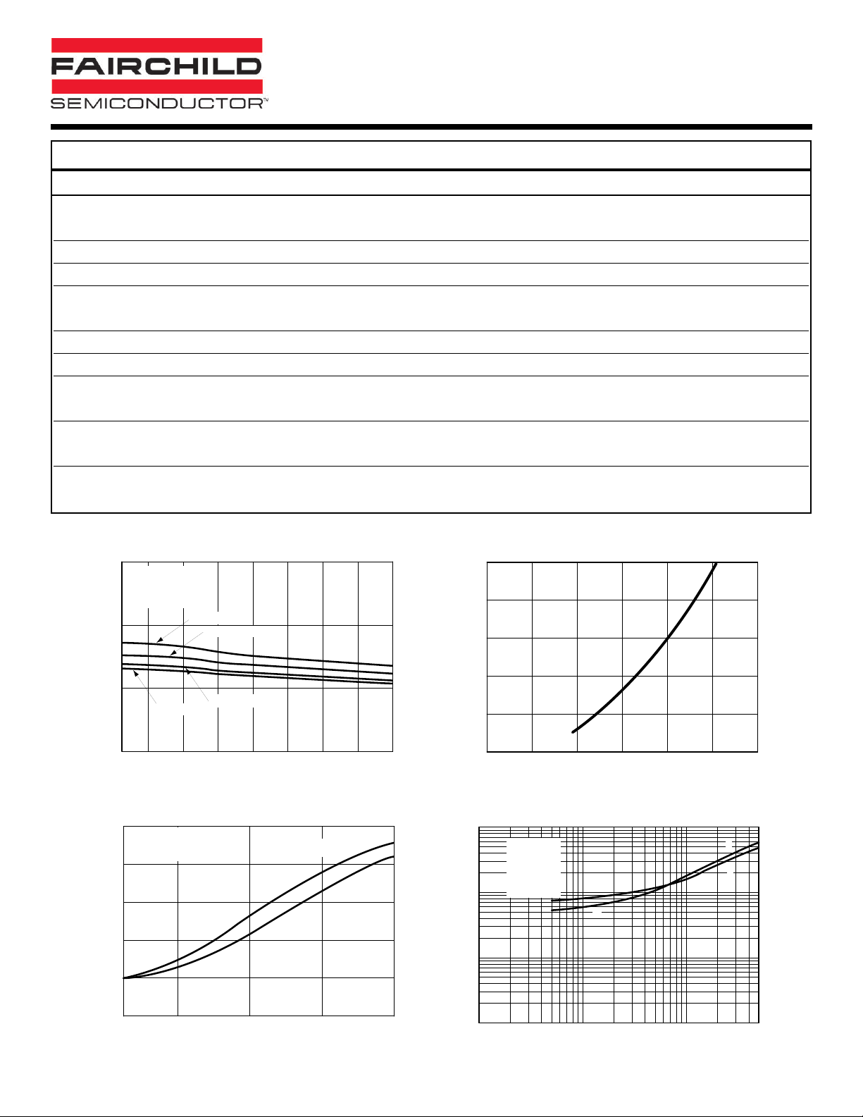
ELECTRICAL / OPTICAL CHARACTERISTICS
(TA= 25°C)
Fig. 1 Forward Voltage vs. Ambient Temperature
3
Pulsed
I
F
Pulse Width = 100 µs
Duty Cycle = 0.1%
I
= 100 mA
2
F
IF = 50 mA
100
T
A
80
60
Fig. 2 Forward Current vs. Forward Voltage
= 25˚C
1
- Forward Voltage (V)
F
V
0
= 10 mA
I
F
-40 -20 0 20 40 60 80 100
IF = 20 mA
TA- Ambient Temperature (
o
C
)
Fig. 3 Collector Emitter Dark Current (Normalized)
4
10
3
10
2
10
1
10
- Normalized Dark Current
CEO
0
I
10
-1
10
Normalized to:
V
CE
T
= 25˚C
A
vs. Ambient Temperature
= 25 V
40 60 80 100
TA-Ambient T emperature (
V
CE
o
C
)
= 25 V
V
= 10 V
CE
40
- Forward Current (mA)
F
I
20
0
1.0 1.1 1.2 1.3 1.4 1.5 1.6
VF - Forward Voltage (V)
Fig. 4 Rise and Fall Time vs. Load Resistance
100
VCC = 5 V
I
= 0.5 mA
C
t
= 100 us
pw
T = 10 ms
T
10
1
Rise and Fall Time (µs)
0.1
10 100 1000
= 25˚C
A
t
f
t
r
RL-Load Resistance (")
t
r
t
f
 Loading...