Fairchild Semiconductor QCK3 Datasheet

PHOTODARLINGTON OPTICAL
INTERRUPTER SWITCH
QCK3 QCK4
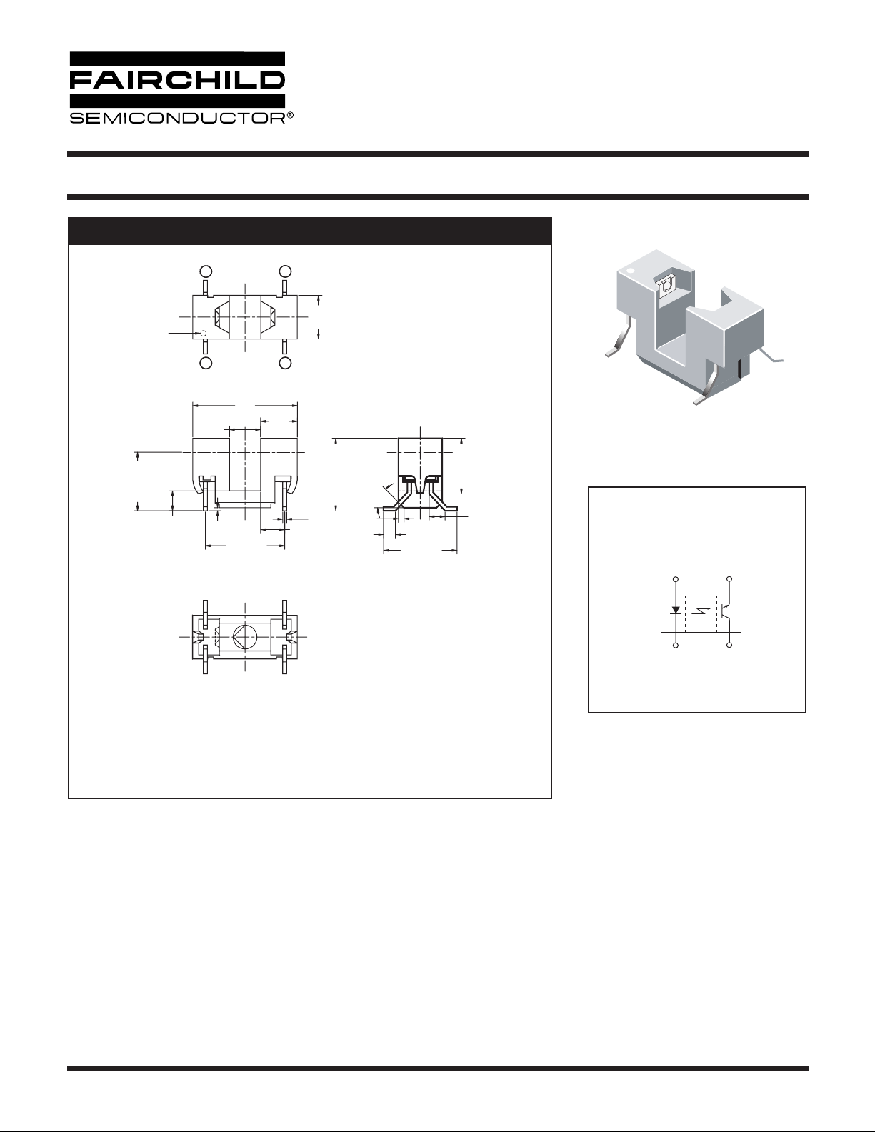
PACKAGE DIMENSIONS
2
C
L
PIN 1
IDENTIFICATIO
N
1
0.527
0.157
OPTICAL C OPTICAL C
L
0.005
0.295±
0.005
0.100±
OPTICAL C
0.015
0.400±
L
C
L
C
L
C
L
0.020
0.185
3
4
0.1215
00
0.22
0.020SQ
(4X)
C
L
PIN 1 CATHODE
PIN 2 ANODE
PIN 3 EMITTER
PIN 4 COLLECTOR
0.020
(4X)
0.365±
0.0283
45.0°
(2X)
L
C
L
0.060±0.020
(4X)
0.020
0.370±
0.280
0.085
(4X)
SCHEMATIC
2
1
3
4
NOTES:
1. Dimensions for all drawings are in inches.
2. Tolerance of ± .010 on all non-nominal dimensions
unless otherwise specified.
3. All leads are coplanar within .006".
4. Housing material is electrically conductive.
DESCRIPTION
The QCK3/QCK4 is a slotted opticalswitch designed for surface mount applications where extreme temperatures are experienced
during solder reflow. The switch consists of a GaAs LED and a silicon photodarlington facing each other across a.157" (4.0 mm)
gap. The leads are formed to sit flush on a PCB during solder reflow.
FEATURES
• Unique single piece housing designed to reduce cost.
• High temperature housing material to withstand extreme temperature.
• Shipped in plastic tubes for protection of leads and to feed automatic placement equipment.
• Sensor package is infrared transparent and tinted to attenuate visible light.
© 2002 Fairchild Semiconductor Corporation
Page 1 of 3
5/13/02

PHOTODARLINGTON OPTICAL
INTERRUPTER SWITCH
QCK3 QCK4
ABSOLUTE MAXIMUM RATINGS
(T
= 25°C unless otherwise specified)
A
Parameter Symbol Rating Units
T
T
T
SOL-F
OPR
STG
-55 to +100 °C
-40 to +85 °C
Operating Temperature
Storage Temperature
Soldering Temperature (Flow)
Preheating Stage for 60 sec 183 °C
Reflow Stage for 5 sec 230 °C
Rate of Temperature Rise 3 to 10 °C/S
EMITTER
Continuous Forward Current
Reverse Voltage
Power Dissipation
(1)
I
F
V
R
P
D
50 mA
6 V
100 mW
SENSOR
V
V
CEO
ECO
I
C
P
D
30 V
6 V
40 mA
150 mW
Collector-Emitter Voltage
Emitter-Collector Voltage
Collector Current
Power Dissipation
(1)
NOTE:
1. Derate power dissipation linearly 1.33 mW/°C above 25°C.
PARAMETER DEVICES TEST CONDITIONS SYMBOL MIN TYP MAX UNITS
EMITTER
Forward Voltage
Reverse Current
= 20 mA V
F
V
= 2 V I
R
F
R
——1.4 V
——100 µA
I
SENSOR
Collector-Emitter Breakdown
Collector-Emitter Leakage
= 1 mA, E
I
C
V
= 5.25 V, E
CE
= 0 BV
e
= 0 I
e
CEO
CEO
30 ——V
——30 µA
COUPLED
On-State Collector Current
QCK3
= 5.0 mA, V
F
= 5 V I
CE
C(ON)
1.0 ——
mA
I
QCK4 3.0 15.0
I
Saturation Voltage
© 2002 Fairchild Semiconductor Corporation
= 5 mA, I
F
= 5.0 mA V
C
Page 2 of 3
CE (SAT)
——1.0 V
5/13/02
 Loading...