

Fairchild Semiconductor MPSA42, MMBTA42, PZTA42 Datasheet
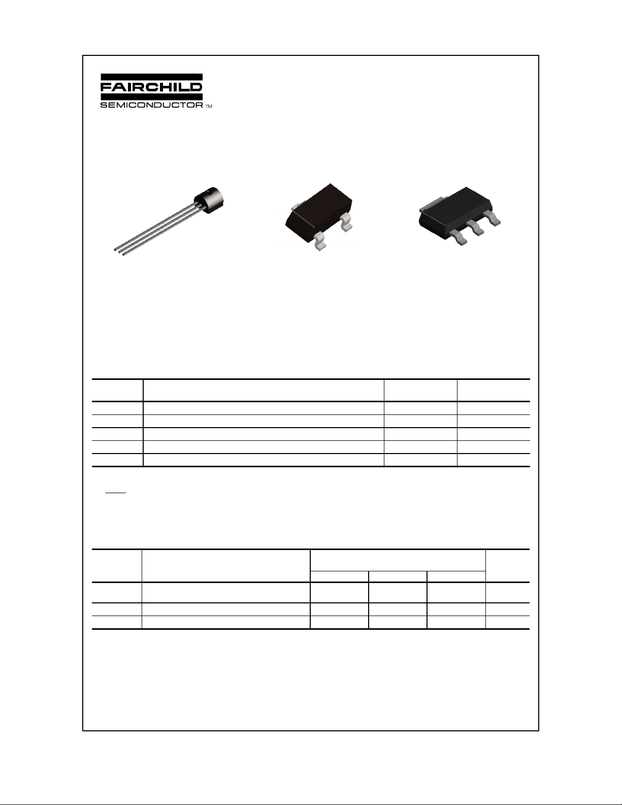
MPSA42 / MMBTA42 / PZTA42
MMBTA42MPSA42
C
E
C
B
E
TO-92
SOT-23
Mark: 1D
B
PZTA42
C
C
B
SOT-223
NPN High Voltage Amplifier
This device is designed for application as a video output to
drive color CRT and other high voltage applications. Sourced
from Process 48.
Absolute Maximum Ratings* TA = 25°C unless otherwise noted
Symbol Parameter Value Units
V
CES
V
CBO
V
EBO
I
C
TJ, T
stg
*These ratings are limiting values above which the serviceability of any semiconductor device may be impaired.
NOTES:
1) These ratings are based on a maximum junction temperature of 150 degrees C.
2) These are steady state limits. The factory should be consulted on applications involving pulsed or low duty cycle operations.
Collector-Emitter V ol tage 300 V
Collector-Base Voltage 300 V
Emitter-Base Volt age 6.0 V
Collector Current - Continuous 500 mA
Operating and Storage Junction Temperature Range -55 to +150
°
C
E
Thermal Characteristics TA = 25°C unless otherwise noted
Symbol Characteristic Max Units
MPSA42 *MMBTA42 **PZTA42
P
D
R
θ
JC
R
θ
JA
*Device mounted on FR-4 PCB 1.6" X 1.6" X 0.06."
**Device mounted on FR-4 PCB 36 mm X 18 mm X 1.5 mm; mounting pad for the collector lead min. 6 cm
2000 Fairchild Semiconductor International
Total Device Dissipation
Derate above 25°C
Ther mal Resistance, Junction to Case 83.3
Thermal Resistance, Junction to Ambient 200 357 125
625
5.0
350
2.8
2
1,000
8.0
.
MPSA42/MMBTA42/PZTA42 Rev A
mW
mW/°C
C/W
°
C/W
°
(BR)
(BR)
(BR)
µ
µ
NPN High Voltage Amplifier
(continued)
Electrical Characteristics TA = 25°C unless otherwise noted
Symbol Parameter Test Conditions Min Max Units
OFF CHARACTERISTICS
V
CEO
V
CBO
V
EBO
I
CBO
I
EBO
ON CHARACTERISTICS*
h
FE
V
CE(
sat
V
sat
BE(
SMALL SIGNAL CHARACTERISTICS
f
T
C
cb
*Pulse Test: Pulse Width ≤ 300 µs, Duty Cycle ≤ 2.0%
Collector-Emitter Breakdown Voltage* IC = 1.0 mA, IB = 0 300 V
Collector-Base Breakdown Voltage
Emitter-Base Breakdown Voltage
I
= 100 µA, IE = 0
C
= 100 µA, IC = 0
I
E
300 V
6.0 V
Collector-Cutoff Current VCB = 200 V, IE = 0 0.1
Emitte r-Cutoff Current VEB = 6.0 V, IC = 0 0.1
DC Current Gain IC = 1.0 mA, VCE = 10 V
I
= 10 mA, VCE = 10 V
C
I
= 30 mA, VCE = 10 V
Collector-Emitter Saturatio n Voltage IC = 20 mA, IB = 2.0 mA 0.5 V
)
Base-Emitter Saturatio n Voltage IC = 20 mA, IB = 2.0 mA 0.9 V
)
C
Current Gain - Bandwidth Product IC = 10 mA, VCE = 20 V,
25
40
40
50 MHz
f = 100 MHz
Collector-Base Capacitance VCB = 20 V, IE = 0, f = 1.0 MHz 3.0 pF
A
A
MPSA42 / MMBTA42 / PZTA42
Spice Model
NPN (Is=34.9f Xti=3 Eg=1.11 Vaf=100 Bf=2.65K Ne=1.708 Ise=16.32p Ikf=23.79m Xtb=1.5 Br=9.769 Nc=2
Isc=0 Ikr=0 Rc=7 Cjc=14.23p Mjc=.5489 Vjc=.75 Fc=.5 Cje=49.62p Mje=.4136 Vje=.75 Tr=934.3p Tf=1.69n
Itf=5 Vtf=20 Xtf=150 Rb=10)
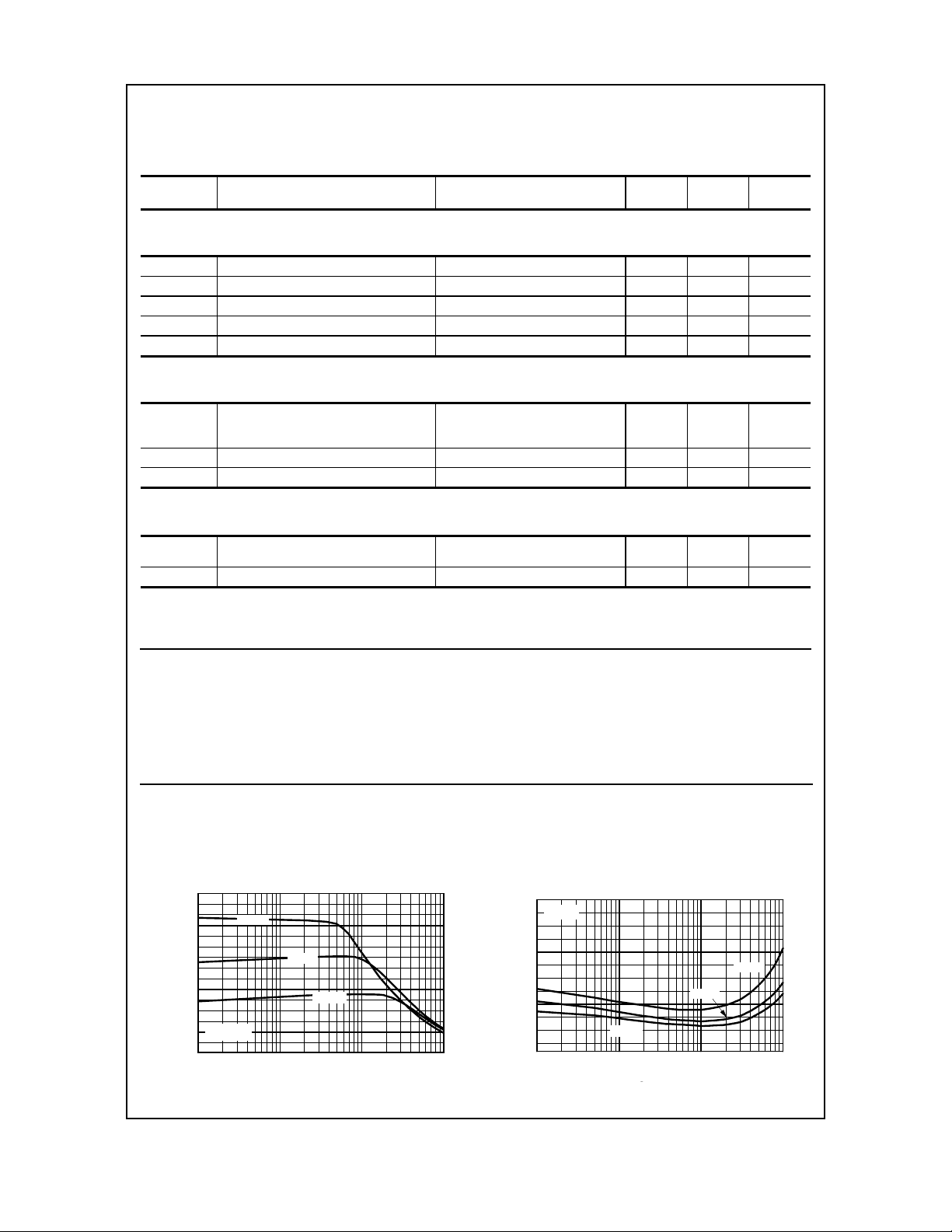
Typical Characteristics
DC Current Gain
vs Collector Current
140
120
100
80
60
40
E
F
20
h - DC CURRENT GAIN
0.1 1 10 100
125 °C
25 °C
- 40 ºC
V = 5V
CE
I - COLLECTOR CURRENT (mA)
C
Collector-Emitter Saturation
Voltage vs Collector Current
0.3
= 10
β
0.25
0.2
0.15
0.1
0.05
0.1 1 10 100
CESAT
V - COLLECTOR-EMITTER VOLTAGE (V)
- 40 ºC
I - COLLECTOR CURRENT (mA)
C
25 °C
125 °C
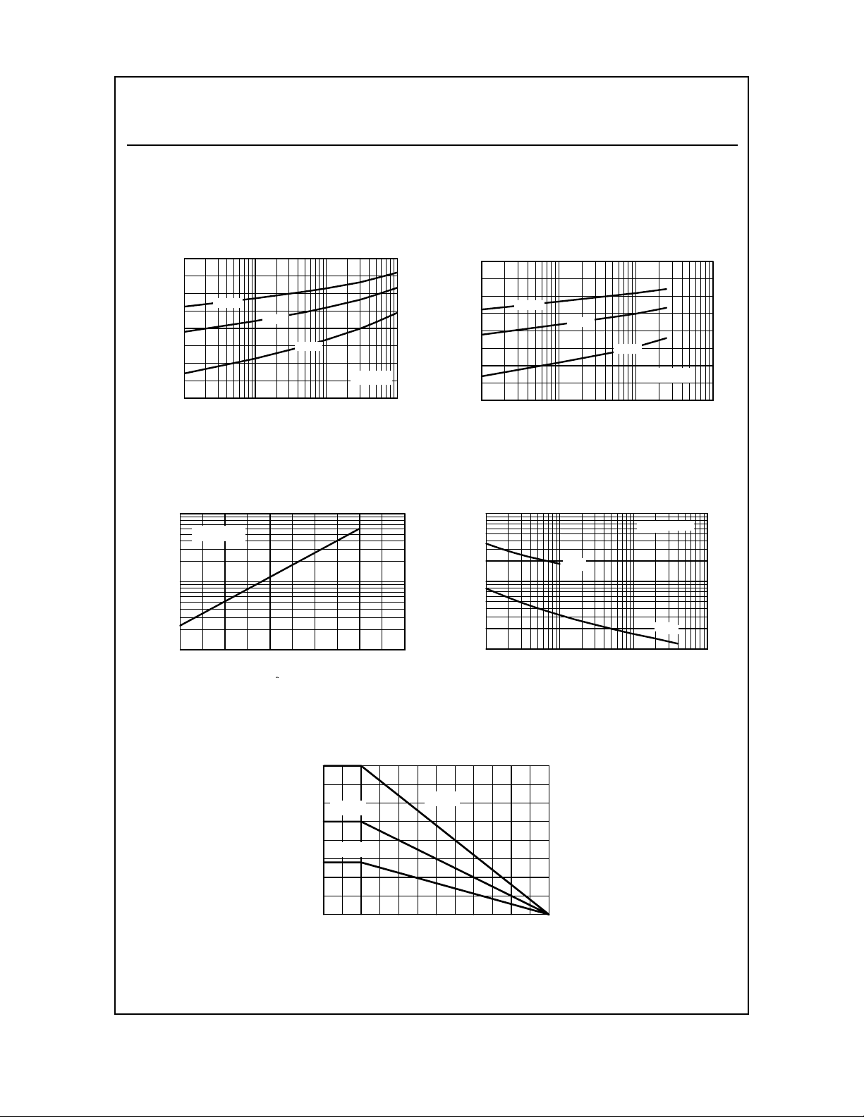
Typical Characteristics (continued)
MPSA42 / MMBTA42 / PZTA42
NPN High Voltage Amplifier
(continued)
Base-Emitter Saturation
Voltage vs Collector Current
1
0.8
0.6
- 40 ºC
25 °C
125 °C
0.4
β
0.2
BESAT
V - BASE-EMITTER VOLTAGE (V)
0.1 1 10 100
I - COLLECTOR CURRENT (mA)
C
Collector-Cuto ff Current
vs Ambient Temperature
100
V = 150V
CB
10
CBO
1
I - COLLECTOR CURRENT (nA)
25 50 75 100 125 150
T - AMBIENT TEMPERATURE ( C)
A
º
= 10
Base-Emitter ON Voltage vs
Collector Current
1
0.8
0.6
0.4
0.2
BE(ON)
V - BASE-EMITTER ON VOLTAGE (V)
- 40 ºC
25 °C
125 °C
V = 1V
CE
0.1 1 10 100
I - COLLECTOR CURRENT (mA)
C
Collector-Base and Emitter-Base
Capacitance vs Reverse Bias Voltage
100
50
20
10
5
CAPACITANCE (pF)
2
1
1 10 100 1000
C
eb
REVERSE BIAS VOLTAGE (V)
T = 25 °C
A
C
cb
Power Dissipation vs
Ambient Temperature
1
0.75
TO-92
0.5
SOT-23
0.25
D
P - POWER DISSIPATION (W)
0
0 255075100125150
SOT-223
TEMPERATURE ( C)
o
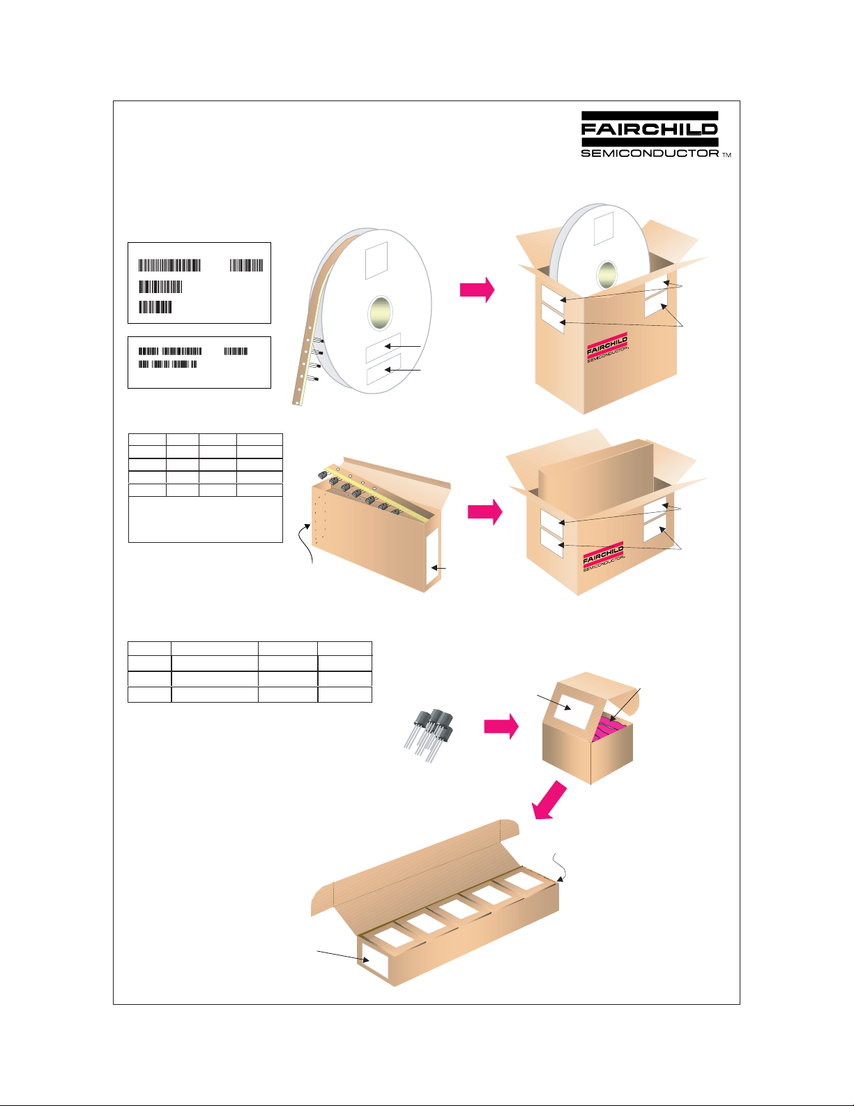
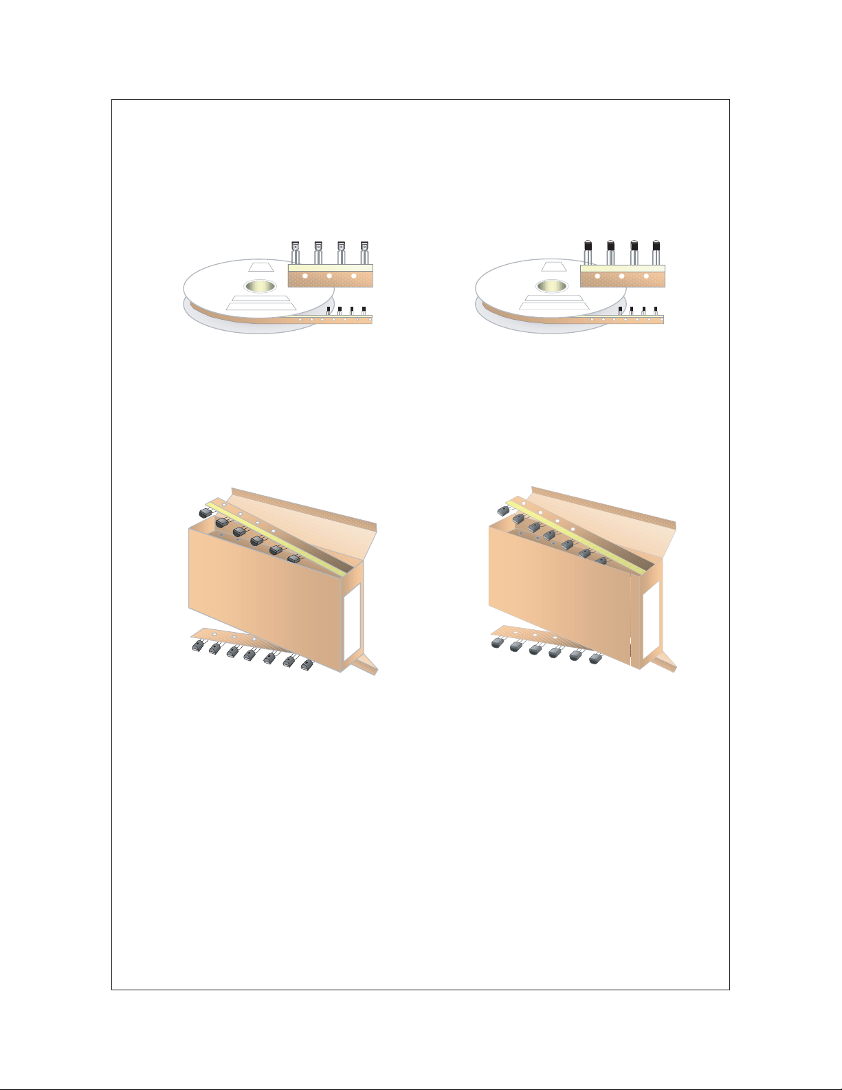
TO-92 Tape and Reel Data and Package Dimensions
TO-92 Packaging
Configuration: Figure 1.0
FSCINT Label sample
FAIRCHILD SEMICONDUCTOR CORPORATION
LOT:
CBVK741B019
NSID:
PN2222N
D/C1:
SPEC REV:
D9842
QA REV:
HTB:B
QTY:
10000
SPEC:
B2
(FSCINT)
F63TNR Label sample
LOT: CBVK741B019
FSID: PN222N
D/C1: D9842 QTY1: SPEC REV:
D/C2: QTY2: CPN:
QTY: 2000
SPEC:
N/F: F (F63TNR)3
TO-92 TNR/AMMO PACKING INFROMATION
Packing Style Quantity EOL code
Reel A 2,000 D26Z
Ammo M 2,000 D74Z
Unit w eight = 0.22 gm
Reel weight with components = 1.04 kg
Amm o weight with componen ts = 1.02 kg
Max q uantity per intermediate box = 10,000 u n its
E2,000 D27Z
P2,000 D75Z
(TO-92) BULK PACKING INFORMATION
EOL
CODE
J18Z
J05Z
NO EOL
CODE
DESCRIPTION
TO-18 OPTION STD NO LEAD CLIP
TO-5 OPTION STD NO LEAD CLIP
TO-92 STANDARD
STRAIGHT
NO LEADCLIP
LEADCLIP
DIMENSION
327mm x 158mm x 135mm
Immediate Box
Customized
Label
QUANTITY
2.0 K / BOX
1.5 K / BOX
2.0 K / BOX
TAPE and REEL OPTION
See Fig 2.0 for various
Reeling Styles
5 Reels per
Intermediate Box
F63TNR
Label
Customized
Label
AMMO PACK OPTION
See Fig 3.0 for 2 Ammo
Pack Options
5 Ammo boxes per
Intermediate Box
F63TNR
Label
BULK OPTION
See Bulk Packing
Information table
FSCINT Label
375mm x 267mm x 375mm
Intermediate Box
333mm x 231mm x 183mm
Intermediate Box
Anti-static
Bubble Sheets
FSCINT
Label
Customized
Label
FSCINT
Label
Customized
Label
530mm x 130mm x 83mm
FSCINT Label
Intermediate box
2000 units per
EO70 box for
std option
C
Label
10,000 units maximum
per intermediate box
for std option
ustomized
5 EO70 boxes per
intermediate Box
114mm x 102mm x 51mm
Immediate Box
September 1999, Rev. B
TO-92 Tape and Reel Data and Package Dimensions, continued
TO-92 Reeling Style
Configuration: Figure 2.0
Machine Option “A” (H)
Style “A”, D26Z, D70Z (s/h )
TO-92 Radial Ammo Packaging
Configuration: Figure 3.0
FIRST WIRE OFF IS COLLECTOR
ADHESIVE TAPE IS ON THE TOP SIDE
FLAT OF TRANSISTOR IS ON TOP
ORDER STYLE
D74Z (M)
Machine Option “E” (J)
Style “E”, D27 Z, D71 Z (s/ h)
FIRST WIRE OFF IS EMITTER
ADHESIVE TAPE IS ON THE TOP SIDE
FLAT OF TRANSISTOR IS ON BOTTOM
ORDER STYLE
D75Z (P)
FIRST WIRE OFF IS EMITTER (ON PKG. 92)
ADHESIVE TAPE IS ON BOTTOM SIDE
FLAT OF TRANSISTOR IS ON BOTTOM
FIRST WIRE OFF IS COLLECTOR (ON PKG. 92)
ADHESIVE TAPE IS ON BOTTOM SIDE
FLAT OF TRANSISTOR IS ON TOP
September 1999, Rev. B
 Loading...