MPSA27/PZTA27
MPSA27/PZTA27
NPN General Purpose Amplifier
• This device is designed for applications requiring
4
extremely high current gain at collector currents to
500mA.
• Sourced from process 03.
• See MPSA28 for characteristics.
Absolute Maximum Ratings* T
1
1. Emitter 2. Base 3. Collector
=25°C unless otherwise noted
A
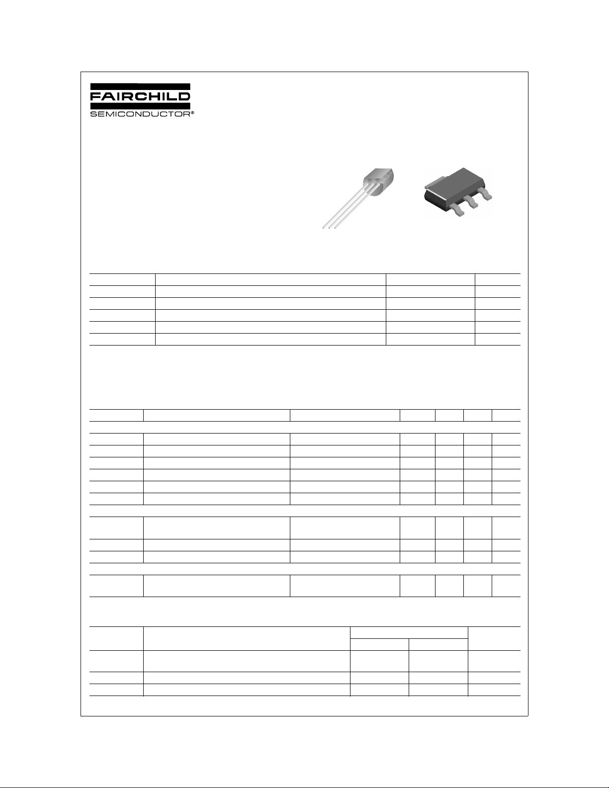
TO-92
1. Base 2. Collector 3. Emitter
1
2
SOT-223
Symbol Parameter Value Units
V
CES
V
CBO
V
EBO
I
C
, T
T
J
stg
* These ratings are limiting values above which the serviceability of any semiconductor device may be impaired.
NOTES:
1) These ratings are based on maximum junction temperature of 150 degrees C.
2) These are steady state limits. The factory should be consulted on applications involving pulsed or low duty cycle operations.
Electrical Characteristics
Collector-Emitter Voltage 60 V
Collector-Base Voltage 60 V
Emitter-Base Voltage 10 V
Collector current - Continuous 800 mA
Operating and Storage Junction Temperature -55 ~ +150 °C
TA=25°C unless otherwise noted
Symbol Parameter Test Condition Min. Typ. Max. Units
Off Characteristics
V
(BR)CES
V
(BR)CBO
V
(BR)EBO
I
CBO
I
CES
I
EBO
Collector-Emitter Breakdown Voltage IC = 100µA, VBE = 0 60 V
Collector-Base Breakdown Voltage IC = 10µA, IC = 0 60 V
Emitter-Base Breakdown Voltage IC = 100µA, IC = 0 10 V
Collector Cutoff Current VCB = 50V, IE = 0 100 nA
Collector Cutoff Current VCE = 50V, VBE = 0 500 nA
Emitter Cutoff Current VEB = 10V, IC = 0 100 nA
On Characteristics
h
FE
V
CE(sat)
V
BE(on)
DC Current Gain IC = 10mA, VCE = 5.0V
= 100mA, VCE = 5.0V
I
C
Collector-Emitter Saturation Voltage IC = 100mA, IB = 0.1mA 1.5 V
Base-Emitter On Voltage IC = 100mA, VCE = 5.0V 2.0 V
10000
10000
Small Signal Characteristics
f
T
Current Gain Bandwidth Product IC = 10mA, VCE = 5.0V,
125 MHz
f = 100MHz
3
Thermal Characteristics
Symbol Parameter
P
D
R
θJC
R
θJA
* Device mounted on FR-4 PCB 36mm × 18mm × 1.5mm: mounting pad for the collector lead min. 6cm.
©2002 Fairchild Semiconductor Corporation Rev. A1, June 2002
Total Device Dissipation
Derate above 25°C
Thermal Resistance, Junction to Case 83.3 °C/W
Thermal Resistance, Junction to Ambient 200 125 °C/W
TA=25°C unless otherwise noted
Max.
MPSA27 *PZTA2 7
625
5.0
1000
8.0
Units
mW
mW/°C

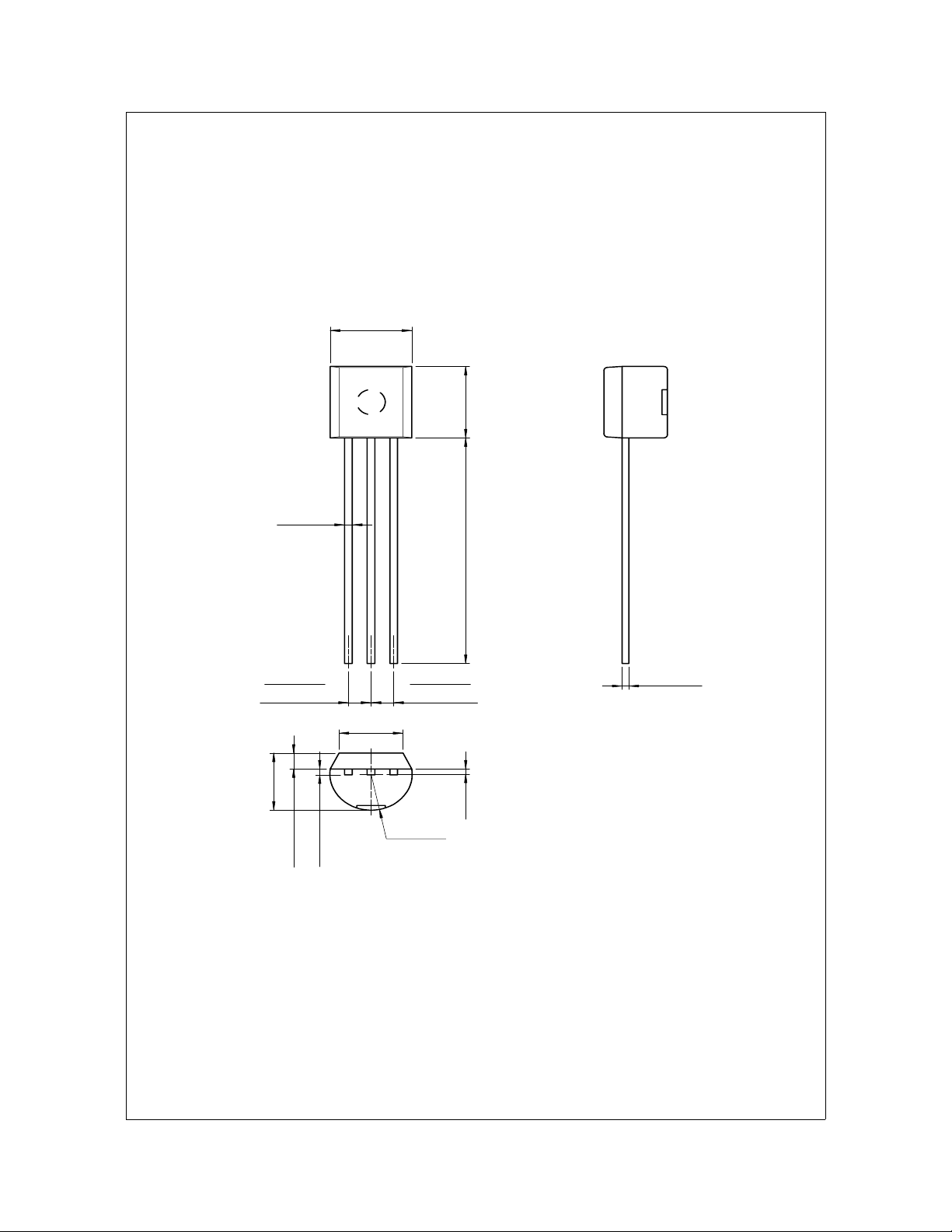
Package Dimensions
0.46
±0.10
4.58
+0.25
–0.15
MPSA27/PZTA27
TO-92
±0.20
4.58
±0.40
1.27TYP
[1.27
±0.20
3.86MAX
±0.10
1.02
+0.10
–0.05
0.38
14.47
1.27TYP
]
3.60
±0.20
[1.27
±0.20
]
0.38
+0.10
–0.05
(0.25)
(R2.29)
Dimensions in Millimeters
©2002 Fairchild Semiconductor Corporation Rev. A1, June 2002
 Loading...