

Fairchild Semiconductor PN5432, PN5434 Datasheet
PN5432
PN5433
PN5434
PN5432 / PN5433 / PN5434
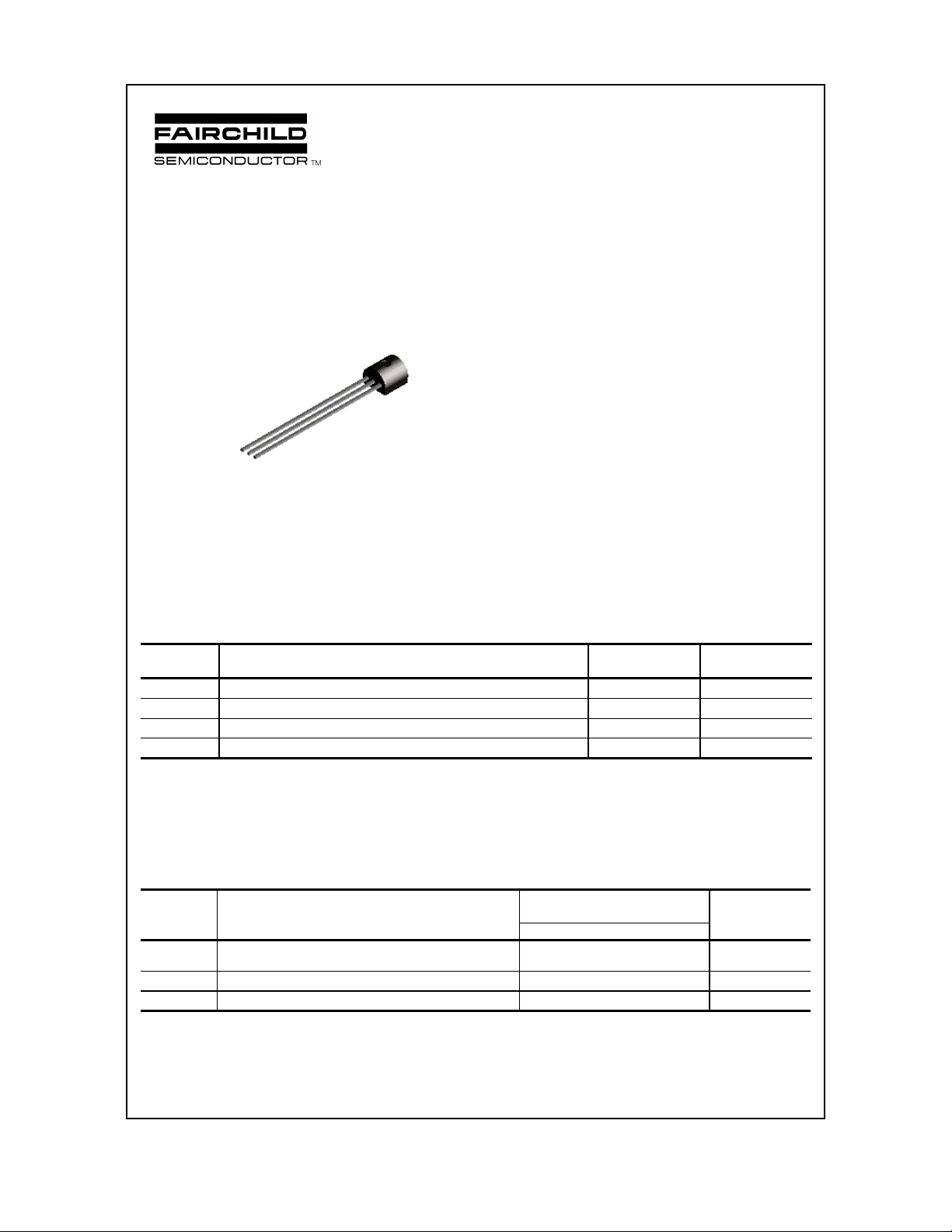
G
S
D
TO-92
N-Channel Switch
This device is designed for analog or digital switching applications where
very low On Resistance is mandatory. Sourced from Process 58. See
J108 for characteristics.
Absolute Maximum Ratings* TA = 25°C unless otherwise noted
Symbol Parameter Value Units
V
DG
V
GS
I
GF
TJ, T
stg
*These ratings are limiting values above which the serviceability of any semiconductor device may be impaired.
NOTES:
1) These ratings are based on a maximum junction temperature of 150 degrees C.
2) These are steady state limits. The factory should be consulted on applications involving pulsed or low duty cycle operations.
Thermal Characteristics TA = 25°C unless otherwise noted
Drain-Gate Voltage 25 V
Gate-Source Voltage -25 V
Forward Gate Current 10 mA
Operating and Stora ge Junction Temperature Range -55 to +150
°
C
Symbol Characteristic Max Units
PN5432 / 5433 / 5434
P
D
R
θ
JC
R
θ
JA
2001 Fairchild Semiconductor Corporation
Total Device Dissipation
Derate above 25°C
Ther mal Resistance , Junct ion to Case 125
Thermal Resistance, Junction to Ambient 357
350
2.8
PN5432/PN5433/PN5434, Rev B
mW
mW/°C
C/W
°
C/W
°

N-Channel Switch
(
(continued)
Electrical Characteristics TA = 25°C unless otherwise noted
Symbol Parameter Test Conditions Min Max Units
OFF CHARACTERISTICS
V
(BR)GSS
I
GSS
I
D(off)
V
GS(off)
ON CHARACTERISTICS
I
DSS
V
DS(on)
r
DS(on)
Gate-Source Breakdown Voltage
I
= 1.0 µA, VDS = 0
G
Gate Reverse Current VGS = 15 V, VDS = 0
= 15 V, VDS = 0, TA = 150 °C
V
GS
Drain Cutoff Leakage Voltage VGS = 10 V, VDS = 5.0 V
= 10 V, VDS = 5.0 V,
V
GS
= 150 °C
T
A
Gate-Source Cutoff Voltage VDS = 5.0 V, ID = 3.0 nA
5433
5434
Zero-Gate Voltage Drain Current* VDS = 15 V, VGS = 0
5433
5434
Drain-Source On Voltage ID = 10 mA, VGS = 0
5433
5434
Drain-Sour ce On Resistance I
= 10 mA, V
D
= 0
GS
5433
5434
I
= 0, VGS = 0, f = 1.0 kHz
D
5433
5434
5432
5432
5432
5432
5432
-25 V
-200
-200
-200
-200
-4.0
-3.0
-1.0
-10
-9.0
-4.0
150
100
30
50
70
100
2.0
5.0
7.0
10
2.0
5.0
7.0
10
pA
nA
pA
nA
V
V
V
mA
mA
mA
mV
mV
mV
Ω
Ω
Ω
Ω
Ω
Ω
PN5432 / PN5433 / PN5434
SMALL SIGNAL CHARACTERISTICS
C
iss
C
rss
Input Capacitance VDS = 0 , V
Reverse Transfer Capacitance VDS = 0 , V
SWITCHING CHARACTERISTICS
t
d
t
r
t
s
t
f
Delay Time
Rise Time
Storage Time
Fall Time
*Pulse Test: Pulse Width ≤ 300 µs, Duty Cycle ≤ 2.0%
= 10 V, f = 1.0 MHz 30 pF
GS
= 10 V, f = 1.0 MHz 15 pF
GS
V
= 1.5 V, V
DD
I
D(on)
V
GS(off)
V
DS(on)
V
DS(on)
V
DS(on)
V
GS
= 10 mA
off)
GS(on)
= 12 V,
= 50 mV 5432
= 70 mV 5433
= 100 mV 5434
= 12 V
= 0,
4.0 ns
1.0 ns
6.0
6.0
6.0
30 ns
ns
ns
ns

TO-92 Tape and Reel Data
TO-92 Packaging
Configuration: Figure 1.0
FSCINT Label sample
FAIRCHILD SEMICONDUCTOR CORPORATION
LOT:
CBVK741B019
NSID:
PN2222N
D/C1:
SPEC REV:
D9842
QA REV:
HTB:B
QTY:
10000
SPEC:
B2
(FSCINT)
F63TNR Label sample
LOT: CBVK741B019
FSID: PN222N
D/C1: D9842 QTY1: SPEC REV:
D/C2: QTY2: CPN:
QTY: 2000
SPEC:
N/F: F (F63TNR)3
TO-92 TNR/AMMO PACKING INFROMATION
Packing Style Quantity EOL cod e
Reel A 2,000 D26Z
E2,000 D27Z
Ammo M 2,000 D74Z
P2,000 D75Z
Unit w eight = 0.22 gm
Reel weight with compo nents = 1 .0 4 kg
Amm o weig ht with components = 1.02 kg
Max q uantity p er interme d iate box = 10,000 units
(TO-92) BULK PACKING INFORMATION
EOL
CODE
J18Z
J05Z
NO EOL
CODE
L34Z
DESCRIPTION
TO-18 OPTION STD NO LEAD CLIP
TO-5 OPTION STD NO LEAD CLIP
TO-92 STANDARD
STRAIGHT FOR: PKG 92,
94 (NON PROELECTRON
SERIES), 96
TO-92 STANDARD
STRAIGHT FOR: PKG 94
(PROELECTRON SERIES
BCXXX, BFXXX, BSRXXX),
97, 98
NO LEADCLIP
NO LEADCLIP
LEADCLIP
DIMENSION
327mm x 158mm x 135mm
Immediate Box
Customized
Label
QUANTITY
2.0 K / BOX
1.5 K / BOX
2.0 K / BOX
2.0 K / BOX
TAPE and REEL OPTION
See Fig 2.0 for various
Reeling Styles
5 Reels per
Intermediate Box
F63TNR
Label
Customized
Label
AMMO PACK OPTION
See Fig 3.0 for 2 Ammo
Pack Options
5 Ammo boxes per
Intermediate Box
F63TNR
Label
BULK OPTION
See Bulk Packing
Information table
FSCINT Label
2000 units per
EO70 box for
std option
375mm x 267mm x 375mm
Intermediate Box
333mm x 231mm x 183mm
Intermediate Box
Anti-static
Bubble Sheets
114mm x 102mm x 51mm
FSCINT
Label
Customized
Label
FSCINT
Label
Customized
Label
Immediate Box
530mm x 130mm x 83mm
FSCINT Label
©2001 Fairchild Semiconductor Corporation
Intermediate box
ustomized
C
Label
10,000 units maximum
per intermediate box
for std option
5 EO70 boxes per
intermediate Box
March 2001, Rev. B1
 Loading...