

Fairchild Semiconductor PN4275 Datasheet
PN4275
PN4275
Discrete POWER & Signal
Technologies
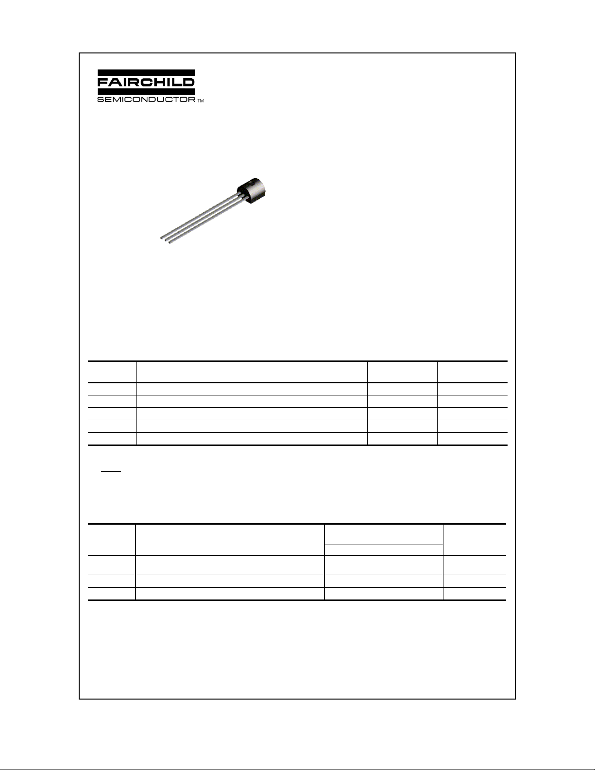
C
B
E
TO-92
NPN Switching Transistor
This device is designed for high speed saturated switching
applications at currents to 100 mA. Sourced from Process 21.
See PN2369A for characteristics.
Absolute Maximum Ratings* TA = 25°C unless otherwise noted
Symbol Parameter Value Units
V
CEO
V
CBO
V
EBO
I
C
TJ, T
stg
*These ratings are limiting values above which the serviceability of any semiconductor device may be impaired.
NOTES:
1) These ratings are based on a maximum junction temperature of 150 degrees C.
2) These are steady state limits. The factory should be consulted on applications involving pulsed or low duty cycle operations.
Thermal Characteristics TA = 25°C unless otherwise noted
Collector-Emitter Voltage 15 V
Collector-Base Voltage 40 V
Em i t ter - Bas e V olt ag e 4. 5 V
Collector Current - Continuous 200 mA
Operating and Storage Junction Temperature Range -55 to +150
°C
Symbol Characteri st ic Max Units
PN4275
P
D
R
θ
JC
R
θ
JA
1997 Fairchild Semiconductor Corporation
Total De vice Dissip at i on
Derate above 25°C
Thermal Resistance, Junction to Case 125 °C/W
Thermal Resistance, Junction to Ambient 357
350
2.8
mW
mW/°C
°C/W
NPN Switching Transistor
(continued)
Electrical Characteristics TA = 25°C unless otherwise noted
Symbol Parameter Test Conditions Min Max Units
OFF CHARACTERISTICS
V
(BR)CEO
V
(BR)CBO
V
(BR)EBO
V
(BR)CES
I
B
I
CBO
ON CHARACTERISTICS*
h
FE
V
sat
CE(
V
sat
BE(
Collector-Emitter Breakdown Voltage* IC = 10 mA, IB = 015V
C oll ec t or -Base Breakd ow n Volt age IC = 10 µA, IE = 0 40 V
Em i t ter - Bas e B r e akdown Vol tage
= 10 µA, IC = 0
I
E
4.5 V
Collector-Emitter Breakdown Voltage IC = 10 µA, IB = 0 40 V
Base Cutoff Current VCE = 20 V 0.4
Colle c tor Cu tof f Cu r ren t VCB = 20 V, IE = 0,
= 65 °C
T
A
DC Cu r re n t Ga in IC = 10 mA, VCE = 1.0 V
= 30 mA, VCE = 0.4 V
I
C
= 100 mA, VCE = 1.0 V
I
Collector-Emitter Saturation Voltage IC = 10 mA, IB = 1.0 mA
)
C
= 30 mA, IB = 3.0 mA
I
C
= 10 mA, IB = 3.3 mA
I
C
IC = 100 mA, IB = 10 mA
= 10 mA, IB = 1.0 mA,
I
C
= 65 °C
T
Base- Emi tt er Saturation Voltage IC = 10 mA, IB = 1.0 mA
)
A
IC = 30 mA, IB = 3.0 mA
= 10 mA, IB = 3.3 mA
I
C
= 100 mA, IB = 10 mA
I
C
35
30
18
0.72
0.74
10
120
0.20
0.25
0.18
0.50
0.30
0.85
1.15
1.0
1.6
µ
A
µ
A
V
V
V
V
V
V
V
V
V
PN4275
SMALL SIGNAL CHARACTERISTICS
C
ob
h
fe
Output Capacitance VCB = 5.0 V, f = 1.0 MHz 4.0 pF
Small-Signal Current Gain IC = 10 mA, VCE = 10 V,
SWITCHING CHARACTERISTICS
t
on
t
d
t
r
t
off
t
s
t
f
t
s
Turn-on Time VCC = 3.0 V, IC = 10 mA, 12 ns
De la y Ti m e IB1 = 3.3 mA, 9.0 ns
Rise Time
Turn-off Time VCC = 3.0 V, IC = 10 mA 12 ns
St or age Tim e IB1 = IB2 = 3.3 mA 8.0 ns
Fall Time
St or age Tim e IC = IB1 = IB2 = 10 mA 13 ns
*Pulse Test: Pulse Width ≤ 300 µs, Duty Cycle ≤ 2.0%
f = 100 MHz
V
= -3.0 V
BE (off)
= -3.0 V
V
BE (off)
4.0
7.0 ns
8.0 ns
 Loading...