

Fairchild Semiconductor PN3645 Datasheet
PN3645
PN3645
Discrete POWER & Signal
Technologies
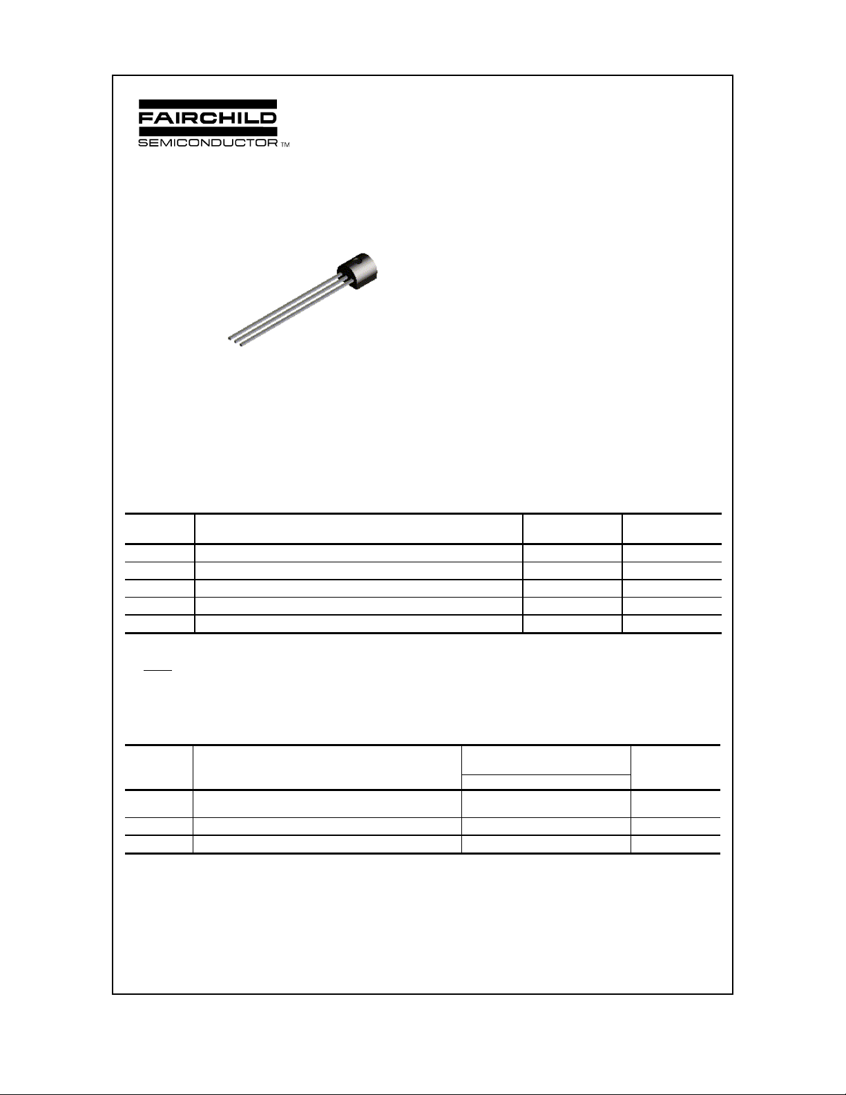
C
B
E
TO-92
PNP General Purpose Amplifier
This device is designed for use as general purpose amplifiers
and switches requiring collector currents to 500 mA. Sourced
from Process 63. See PN2907A for characteristics.
Absolute Maximum Ratings* TA = 25°C unless otherwise noted
Symbol Parameter Value Units
V
CEO
V
CBO
V
EBO
I
C
TJ, T
stg
*These ratings are limiting values above which the serviceability of any semiconductor device may be impaired.
NOTES:
1) These ratings are based on a maximum junction temperature of 150 degrees C.
2) These are steady state limits. The factory should be consulted on applications involving pulsed or low duty cycle operations.
Thermal Characteristics TA = 25°C unless otherwise noted
Collector-Emitter Voltage 60 V
Collector-Base Voltage 60 V
Emitter-Base Voltage 5.0 V
Collector Current - Continuous 800 mA
Operating and Storage Junction Temperature Range -55 to +150
°C
Symbol Characteristi c Max Units
PN3645
P
D
R
θ
JC
R
θ
JA
1997 Fairchild Semiconductor Corporation
Total Device Dissipation
Derate above 25°C
Thermal Resistance, Junction to Case 83.3 °
Thermal Resistance, Junction to Ambient 200
625
5.0
mW
mW/°C
C/W
°C/W
PNP General Purpose Amplifier
(continued)
Electrical Characteristics TA = 25°C unless otherwise noted
Symbol Parameter Test Conditions Min Max Units
OFF CHARACTERISTICS
V
(BR)CEO
V
(BR)CBO
V
(BR)EBO
I
CES
I
BL
ON CHARACTERISTICS*
h
FE
V
sat
CE(
V
sat
BE(
Collector-Emitter Breakdown
IC = 10 mA, IB = 0 60 V
Voltage*
Collector-Base Breakdown Voltage
Emitter-Base Breakdown Voltage
= 100 µA, IE = 0
I
C
= 10 µA, IC = 0
I
E
60 V
5.0 V
Co llecto r-C uto ff Cur rent VCB = 50 V, IE = 0
= 50 V, IE = 0, TA = 65°C
V
CB
Bas e-Cuto f f Current VCE = 50 V, IC = 0 35 nA
DC Current Gain VCE = 10 V, IC = 0.1 mA
= 10 V, IC = 1.0 mA
V
CE
= 10 V, IC = 10 mA
V
CE
VCE = 10 V, IC = 150 mA
= 2.0 V, IC = 300 mA
V
CE
VCE = 1.0 V, IC = 50 mA
Collector-Emitter Saturation Voltage IC = 50 mA, IB = 2.5 mA
)
Base-Emitter Saturation Voltage IC = 50 mA, IB = 2.5 mA
)
= 150 mA, IB = 15 mA
I
C
IC = 150 mA, IB = 15 mA
40
80
100
100
20
80
35
2.0
300
240
0.25
0.4
1.0
1.3
nA
µ
A
V
V
V
V
PN3645
SMALL SIGNAL CHARACTERISTICS
C
ob
C
ib
h
fe
Output Capacitance VCB = 10 V, f = 140 kHz 8.0 pF
Input Capacitance VBE = 0.5 V, f = 140 kHz 35 pF
Small-Signal Current Gain IC = 20 mA , VCE = 20 V,
SWITCHING CHARACTERISTICS
t
on
t
d
t
r
t
off
t
s
t
f
Turn-o n Time VCC = 30 V, IC = 300 mA, 40 ns
Delay Time IB1 = 30 mA 25 ns
Rise Time 35 ns
Turn -off Tim e VCC = 30 V, IC = 300 mA 100 ns
Storage Time IB1 = IB2 = 30 mA 70 ns
Fall Time 50 ns
*Pulse Test: Pulse Width ≤ 300 µs, Duty Cycle ≤ 2.0%
f = 100 MHz
2.0
 Loading...