

Fairchild Semiconductor MPS3563, PN3563MPS3563 Datasheet
NPN RF Amplifier
PN3563
Absolute Maximum Ratings* TA = 25°C unless otherwise noted
*These ratings are limiting values above which the serviceability of any semiconductor device may be impaired.
NOTES:
1) These ratings are based on a maximum junction temperature of 150 degrees C.
2) These are steady state limits. The factory should be consulted on applications involving pulsed or low duty cycle operations.
Thermal Characteristics TA = 25°C unless otherwise noted
This device is designed for use as RF amplifiers, oscillators and
multipliers with collector currents in the 1.0 mA to 30 mA range.
Sourced from Process 43. See PN918 for characteristics.
Symbol Parameter Value Units
V
CEO
Collector-Emitter Voltage 15 V
V
CBO
Collector-Base Voltage 30 V
V
EBO
Em i t ter- Base V oltag e 2. 0 V
I
C
Collector Current - Continuous 50 mA
TJ, T
stg
Operating and Storage Junction Temperature Range -55 to +150
°C
Symbol Characteri st ic Max Units
PN3563
P
D
Total De vice Dissip at i on
Derate above 25°C
350
2.8
mW
mW/°C
R
θ
JC
Thermal Resistance, Junction to Case 125 °C/W
R
θ
JA
Thermal Resistance, Junction to Ambient 357
°C/W
C
B
E
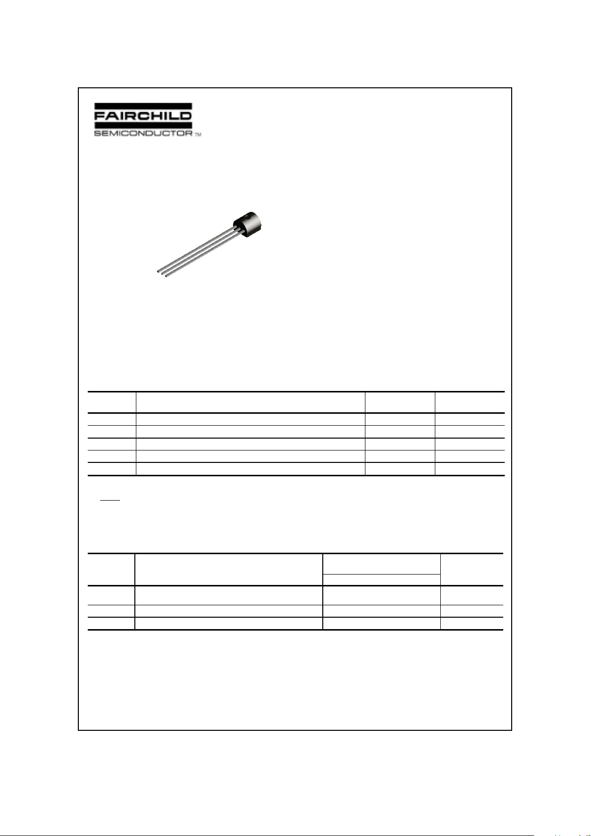
TO-92
PN3563
Discrete POWER & Signal
Technologies
1997 Fairchild Semiconductor Corporation
PN3563
NPN RF Amplifier
(continued)
Electrical Characteristics TA= 25°C unless otherwise noted
OFF CHARACTERISTICS
Symbol Parameter Test Conditions Min Max Units
V
CEO(
sus
)
Collector-Emitter Sustaining Voltage* IC = 3.0 m A, IB = 0 15 V
V
(BR)CBO
Col l e ctor-Base B r eak down Voltag e IC = 100 µA, IE = 0 30 V
V
(BR)EBO
Em i t ter- Base B r e akdown Vol tage
I
E
= 10 µA, IC = 0
2.0 V
I
CBO
Collec t or Cu tof f Curr ent VCB = 15 V, I
E
= 0
V
CB
= 15 V, TA = 150°C
0.05
5.0
µ
A
nA
ON CHARACTERISTICS*
h
FE
DC Curren t Ga in IC = 8.0 m A, VCE = 10 V 20 200
SMALL SIGNAL CHARACTERISTICS
f
T
Current Gain - Bandwidth Product IC = 8.0 m A, VCE = 10 V,
f = 100 MHz
600 1500 MHz
C
obo
Output Capacitance VCB = 10 V, IE = 0, f = 1.0 MHz
VCB = 0, IE = 0, f = 1.0 MHz
1.7
3.0
pF
pF
C
ibo
Input Capacitance VBE = 0.5 V, IC = 0, f = 140 MHz 2.0 pF
h
fe
Small-Signal Current Gain IC = 8.0 m A, VCE = 10 V,
f = 1. 0 kHz
20 250
rb’C
C
Collector Base Time Constant IC = 8.0 m A, VCE = 10 V,
f = 79.8 MHz
8.0 25 pS
FUNCTIONAL TEST
G
pe
Ampl ifier Power Gain IC = 8.0 m A, VCB = 10 V,
f = 20 0 M Hz
14 26 dB
*Pulse Test: Pulse Width ≤ 300 µs, Duty Cycle ≤ 2.0%
 Loading...