

P6KE6.8(C)A - P6KE440(C)A
Features
• Glass passivated junction.
• 600W Peak Pulse Power capability at
1.0 ms.
• Excellent clamping capability.
• Low incremental surge resistance.
• Fast response time; typically less
than 1.0 ps from 0 volts to BV for
unidirectional and 5.0 ns for
bidirectional.
• Typical I
less than 1.0 µA above 10V .
R
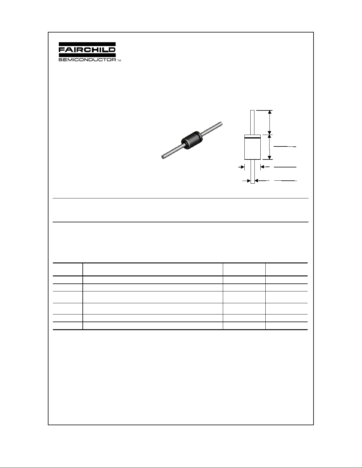
COLOR BAND DENOTES CATHODE
DO-15
EXCEPT BIPOLAR
1.0 min (25.4)
Dimensions in
inches (mm)
0.300 (7.62)
0.230 (5.84)
0.140 (3.56)
0.104 (2.64)
0.034 (0.86)
0.028 (0.71)
P6KE6.8(C)A - P6KE440(C)A
DEVICES FOR BIPOLAR APPLICA TIONS
- Bidirectional types use CA suffix.
- Electrical Characteristics apply in both directions.
600 Watt Transient Voltage Suppressors
Absolute Maximum Ratings* T
Symbol Parameter Value Units
P
PPM
I
PPM
P
D
i
f(surge)
T
stg
T
J
*These ratings are limiting values above which the serviceability of any semiconductor device may be impaired.
Note 1: Measured on 8.3 ms single half-sine wave; Duty cycle = 4 pulses per minute maximum.
Peak Pulse Power Dissipation at TA=25°C, TP=1ms
Peak Pulse Current see table A
Steady State Power Dissipation
.375 " lead length @ T
= 75°C
A
Peak Forward Surge Current
superimposed on rated load (JEDEC method)
Storage Temperature Range -65 to +175
Operating Junction Temperature -65 to +175
= 25°C unless otherwise noted
A
(Note 1)
minimum 600 W
5.0 W
100 A
°
°
C
C
1998 Fairchild Semiconductor Corporation
P6KE6.8(C)A - P6KE440(C)A, Rev. A
Transient Voltage Supressors
(continued)
P6KE6.8(C)A - P6KE440(C)A
Electrical Characteristics T
Uni-directional
Bi-directional (C)
Device
Reverse
Stand-off Voltage
V
(V)
RWM
Breakd own Voltage
V
min max
= 25°C unless otherwise noted
A
BR
(V)
Test
Current
(mA)
IT
Max Clamping
Voltage @IPPM
VC(V)
Max Peak Pulse
Surge Current
I
(A)
PPM
Max Reverse
Leakage V
IR (uA)*
P6KE6.8(C)A 5.80 6.45 7.14 10 10.5 57.1 1000
P6KE7.5(C)A 6.40 7.13 7.88 1 11.3 53.1 500
P6KE8.2(C)A 7.02 7.79 8.61 1 12.1 50.0 200
P6KE9.1(C)A 7.78 8.65 9.55 1 13.4 45.0 50
P6KE10(C)A 8.55 9.50 10.5 1 14.5 41.0 10
P6KE11(C)A 9.4 10.5 11.6 1 15.6 38.0 5
P6KE12(C)A 10.2 11.4 12.6 1 16.7 36.0 5
P6KE13(C)A 11.1 12.4 13.7 1 18.2 33.0 5
P6KE15(C)A 12.8 14.3 15.8 1 21.2 28.0 5
P6KE16(C)A 13.6 15.2 16.8 1 22.5 27.0 5
P6KE18(C)A 15.3 17.1 18.9 1 25.2 24.0 5
P6KE20(C)A 17.1 19.0 21.0 1 27.7 22.0 5
P6KE22(C)A 18.8 20.9 23.1 1 30.6 20.0 5
P6KE24(C)A 20.5 22.8 25.2 1 33.2 18.1 5
P6KE27(C)A 23.1 25.7 28.4 1 37.5 16.0 5
P6KE30(C)A 25.6 28.5 31.5 1 41.4 14.5 5
P6KE33(C)A 28.2 31.4 34.7 1 45.7 13.2 5
P6KE36(C)A 30.8 34.2 37.8 1 49.9 12.0 5
P6KE39(C)A 33.3 37.1 41.0 1 53.9 11.2 5
P6KE43(C)A 36.8 40.9 45.2 1 59.3 10.1 5
P6KE47(C)A 40.2 44.7 49.4 1 64.8 9.3 5
P6KE51(C)A 43.6 48.5 53.6 1 70.1 8.6 5
P6KE56(C)A 47.8 53.2 58.8 1 77.0 7.8 5
P6KE62(C)A 53.0 58.9 65.1 1 85.0 7.1 5
P6KE68(C)A 58.1 64.6 71.4 1 92.0 6.5 5
P6KE75(C)A 64.1 71.3 78.8 1 103.0 5. 8 5
P6KE82(C)A 70.1 77.9 86.1 1 113.0 5. 3 5
P6KE91(C)A 77.8 86.5 95.5 1 125.0 4. 8 5
P6KE100(C)A 85.5 95.0 105.0 1 137.0 4.4 5
P6KE110(C)A 94.0 105.0 116.0 1 152.0 4.0 5
P6KE120(C)A 102.0 114.0 126.0 1 165.0 3.6 5
P6KE130(C)A 111.0 124.0 137.0 1 179.0 3.4 5
P6KE150(C)A 128.0 143.0 158.0 1 207.0 2.9 5
P6KE160(C)A 136.0 152.0 168.0 1 219.0 2.7 5
P6KE170(C)A 145.0 162.0 179.0 1 234.0 2.6 5
P6KE180(C)A 154.0 171.0 189.0 1 246.0 2.4 5
P6KE200(C)A 171.0 190.0 210.0 1 274.0 2.2 5
P6KE220(C)A 185.0 209.0 231.0 1 328.0 1.9 5
P6KE250(C)A 214.0 237.0 263.0 1 344.0 1.8 5
P6KE300(C)A 256.0 285.0 315.0 1 414.0 1.5 5
P6KE350(C)A 300.0 332.0 368.0 1 482.0 1.3 5
P6KE400(C)A 342.0 380.0 420.0 1 548.0 1.1 5
P6KE440(C)A 376.0 418.0 462.0 1 602.0 1.0 5
RWM
* For bidirectional parts with V
<10V, the IR max limit is doubled.
RWM
P6KE6.8(C)A - P6KE440(C)A, Rev. A

T ypical Characteristics
P6KE6.8(C)A - P6KE440(C)A
Transient Voltage Supressors
(continued)
Peak Pulse Power Rating Curve
100
T = 25 C
º
A
10
1
PULSE POWER (kW)
0.1
0.0001 0.001 0.01 0.1 1 10
PULSE WIDTH (ms)
Pulse Waveform
150
tf = 10µsec
Peak Value
100
Ippm
50
PEAK PULSE CURRENT (%)
td
0
01234
T = 25 C
º
A
Pulse Width (td) is Defined
as the Poin t W here the Peak
Current Decays to 50% of Ipp
Half Value-Ipp
2
10/100 0µsec Wa veform
as Defined by R.E.A.
e-kt
TIME (ms)
Pulse Deratin g Curve
100
75
50
PULSE PO WER (%)
25
0
0 25 50 75 100 125 150 175 200
AMBIE N T TEMPERA TURE ( C)
º
Junction Capac i tan ce - Unidirec tional
6000
4000
2000
1000
500
200
100
CAPACITAN CE (p F)
50
Measured at
Stand-Off
Voltage (V mw)
20
10
1 5 10 50 100 200
REVERSE VOLTAGE (V)
T = 25 C
º
A
f = 1.0 MHz
Visg = 50m Vp-p
Measured at
Zero Bias
Steady State Power Derating Curve
5
3.75
2.5
1.25
POWE R DISSIPATION (W)
0
0 25 50 75 100 125 150 175 200
LEAD TE MP ERATU RE ( C)
º
Non-Repetitive Surge Curre nt
200
100
50
20
FORWARD SURGE CURRENT (A)
10
12 51020 50100
NUMBE R OF CY CL E S AT 60Hz
T = T max
A
A
8.3ms Single Half Sine -Wave
JEDEC Method
P6KE6.8(C)A - P6KE440(C)A, Rev. A

DO-15 Package Dimensions
DO-15 (FS PKG Code P2)
1:1
Scale 1:1 on letter size paper
Dimensions shown below are in:
inches [millimeters]
Part Weight per unit (gram): 0.4
1.0 min (25.4)
0.300 (7.62)
0.230 (5.84)
0.140 (3.56)
∅
0.104 (2.64)
0.034 (0.86)
∅
0.028 (0.71)
August 1999, Rev. A

TRADEMARKS
The following are registered and unregistered trademarks Fairchild Semiconductor owns or is authorized to use and is
not intended to be an exhaustive list of all such trademarks.
ACEx™
CoolFET™
CROSSVOLT™
E2CMOS
TM
FACT™
FACT Quiet Series™
®
FAST
FASTr™
GTO™
HiSeC™
ISOPLANAR™
MICROWIRE™
POP™
PowerTrench™
QS™
Quiet Series™
SuperSOT™-3
SuperSOT™-6
SuperSOT™-8
TinyLogic™
UHC™
VCX™
DISCLAIMER
FAIRCHILD SEMICONDUCTOR RESERVES THE RIGHT TO MAKE CHANGES WITHOUT FURTHER
NOTICE TO ANY PRODUCTS HEREIN TO IMPROVE RELIABILITY, FUNCTION OR DESIGN. FAIRCHILD
DOES NOT ASSUME ANY LIABILITY ARISING OUT OF THE APPLICATION OR USE OF ANY PRODUCT
OR CIRCUIT DESCRIBED HEREIN; NEITHER DOES IT CONVEY ANY LICENSE UNDER ITS PATENT
RIGHTS, NOR THE RIGHTS OF OTHERS.
LIFE SUPPORT POLICY
FAIRCHILD’S PRODUCTS ARE NOT AUTHORIZED FOR USE AS CRITICAL COMPONENTS IN LIFE SUPPORT
DEVICES OR SYSTEMS WITHOUT THE EXPRESS WRITTEN APPROV AL OF FAIRCHILD SEMICONDUCTOR CORPORA TION.
As used herein:
1. Life support devices or systems are devices or
systems which, (a) are intended for surgical implant into
the body, or (b) support or sustain life, or (c) whose
failure to perform when properly used in accordance
with instructions for use provided in the labeling, can be
reasonably expected to result in significant injury to the
user.
2. A critical component is any component of a life
support device or system whose failure to perform can
be reasonably expected to cause the failure of the life
support device or system, or to affect its safety or
effectiveness.
PRODUCT STA TUS DEFINITIONS
Definition of Terms
Datasheet Identification Product Status Definition
Advance Information
Preliminary
No Identification Needed
Obsolete
Formative or
In Design
First Production
Full Production
Not In Production
This datasheet contains the design specifications for
product development. Specifications may change in
any manner without notice.
This datasheet contains preliminary data, and
supplementary data will be published at a later date.
Fairchild Semiconductor reserves the right to make
changes at any time without notice in order to improve
design.
This datasheet contains final specifications. Fairchild
Semiconductor reserves the right to make changes at
any time without notice in order to improve design.
This datasheet contains specifications on a product
that has been discontinued by Fairchild semiconductor.
The datasheet is printed for reference information only.
 Loading...