

Fairchild Semiconductor NZT660A, NZT660 Datasheet
July 1998
NZT660/NZT660A
NZT660 / NZT660A
C
E
C
B
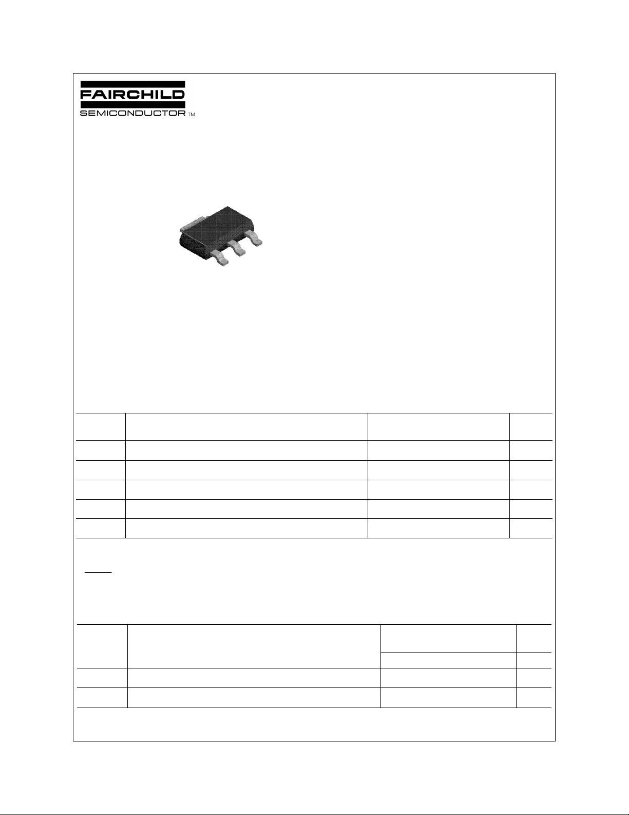
SOT-223
PNP Low Saturation Transistor
These devices are designed with high current gain and low saturation voltage with collector currents up to 3A
continuous.
Absolute Maximum Ratings* T
ParameterSymbol
V
CEO
V
CBO
V
EBO
I
C
T
J, Tstg
*These ratings are limiting values above which the serviceability of any semiconductor device may be impaired.
A = 25°C unless otherwise noted
NZT660/NZT660A
NOTES:
1) These ratings are based on a maximum junction temperature of 150°C.
2) These are steady state limits. The factory should be consulted on applications involving pulsed or low duty cycle operations.
Thermal Characteristics T
Symbol
P
D
R
θJA
A = 25°C unless otherwise noted
Max
Characteristic
NZT660/NZT660A
Units
V60Collector-Emitter Voltage
V80Collector-Base Voltage
V5Emitter-Base Voltage
A3Collector Current - Continuous
°C-55 to +150Operating and Storage Junction Temperature Range
Units
W2Total Device Dissipation
°C/W62.5Thermal Resistance, Junction to Ambient
1998 Fairchild Semiconductor Corporation
Nzt660.lwpPrPA 7/10/98 revC
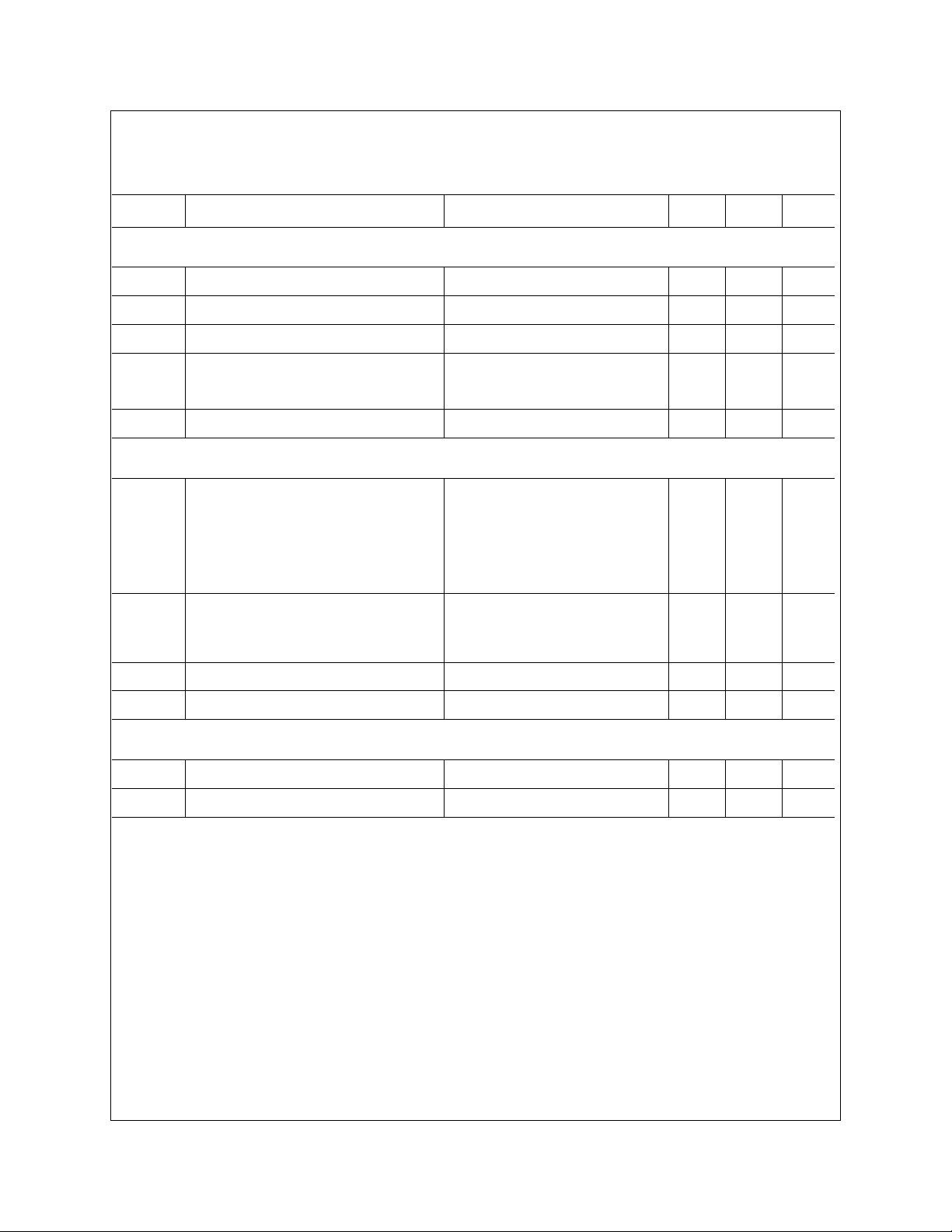
SMALL SIGNAL CHARACTERISTICS
ON
CHARACTERISTICS
OFF CHARACTERISTICS
PNP Low Saturation Transistor
NZT660/NZT660A
(continued)
Electrical Characteristics T
BV
BV
BV
I
CBO
I
EBO
h
FE
V
CE(sat)
V
BE(sat)
V
BE(on)
CEO
CBO
EBO
Collector-Emitter Breakdown Voltage
Collector-Base Breakdown Voltage
Emitter-Base Breakdown Voltage
Collector Cutoff Current
Emitter Cutoff Current
*
DC Current Gain
Collector-Emitter Saturation Voltage
Base-Emitter Saturation Voltage
Base-Emitter On Voltage
A = 25°C unless otherwise noted
= 10 mA
I
C
= 100 µA
I
C
= 100 µA
I
E
V
CB
V
CB
V
EB
= 100 mA, VCE = 2 V
I
C
I
= 500 mA, VCE = 2 V NZT660
C
NZT660A
IC = 1 A, VCE = 2 V
I
= 3 A, VCE = 2 V
C
= 1 A, IB = 100 mA
I
C
I
= 3 A, IB = 300 mA NZT660
C
NZT660A
I
= 1 A, IB = 100 mA
C
= 1 A, VCE = 2 V
I
C
= 30 V
= 30 V, TA=100°C
= 4V
70
100
250
80
25
100
10
100
300
550
550
500
UnitsMaxMinTest ConditionsParameterSymbol
V60
V80
V5
nA
uA
nA
-
mV300
V1.25
V1
C
obo
f
T
*Pulse Test: Pulse Width ≤ 300 µs, Duty Cycle ≤ 2.0%
Output Capacitance
Transition Frequency
= 10 V, IE = 0, f = 1MHz
V
CB
= 100 mA,VCE = 5 V, f=100MHz
I
C
pF45
- 75
Nzt660.lwpPrPA 7/10/98 revC
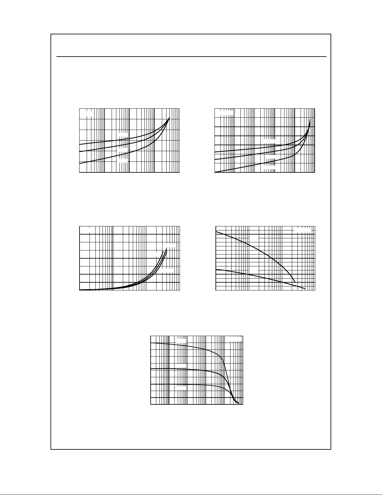
T ypical Characteristics
Base-Emitter Saturation
Voltage v s C ol lector Current
1.4
β = 10
1.2
1
- 40°C
0.8
0.6
0.4
0.2
0.001 0.01 0.1 1 10
T
A
S
E
B
V -BASE-EMITTER SATURATION VOLTAGE(V)
I - COLL ECTOR CURR ENT ( A)
25°C
125°C
C
Collector-Emitter Saturation
Voltage vs Collector Current
0.8
β = 10
0.7
0.6
0.5
0.4
0.3
0.2
0.1
0
0.01 0.1 1 10
CESAT
V - COLLECTOR-EMITTER VOLTAGE (V)
I - COLLECTOR CURRENT (mA)
C
125 °C
25°C
- 40°C
Base-Emitter On Voltage vs.
Collector Current
1.6
V = 2.0V
ce
1.4
1.2
1
0.8
0.6
0.4
0.2
BEON
0.0001 0.001 0. 01 0.1 1 10
V - BA SE -EM ITTER O N VOLTAGE (V)
I - COL LE C T O R CURRE NT ( A)
C
- 40°C
25°C
125°C
Input/Output Capacit ance vs.
Reverse Bias Voltage
400
350
300
C
obo
250
200
150
100
CAPACITANCE (pf)
C
ibo
50
0
0.1 0.5 1 10 20 50 100
V - COLLE CT OR VOLTAGE (V)
CE
V = 2.0V
f = 1.0MH z
ce
Current Gain vs. Collector Current
1000
900
125°C
800
700
600
500
25°C
400
300
FE
H - CURRENT GAIN
200
- 40°C
100
0
0.0001 0.001 0.01 0.1 1 10
I - COLLECTOR CUR RENT (mA)
C
V = 2.0V
ce
PA
 Loading...