

Fairchild Semiconductor NMC27C64N200, NMC27C64NE200, NMC27C64Q150, NMC27C64Q250, NMC27C64QE200 Datasheet
...
1
www.fairchildsemi.com
NMC27C64 Rev. C
NMC27C64 65,536-Bit (8192 x 8) CMOS EPROM
NMC27C64
65,536-Bit (8192 x 8) CMOS EPROM
General Description
The NMC27C64 is a 64K UV erasable, electrically reprogrammable
and one-time programmable (OTP) CMOS EPROM ideally suited
for applications where fast turnaround, pattern experimentation
and low power consumption are important requirements.
The NMC27C64 is designed to operate with a single +5V power
supply with ±10% tolerance. The CMOS design allows the part to
operate over extended and military temperature ranges.
The NMC27C64Q is packaged in a 28-pin dual-in-line package
with a quartz window. The quartz window allows the user to
expose the chip to ultraviolet light to erase the bit pattern. A new
pattern can then be written electrically into the device by following
the programming procedure.
The NMC27C64N is packaged in a 28-pin dual-in-line plastic
molded package without a transparent lid. This part is ideally
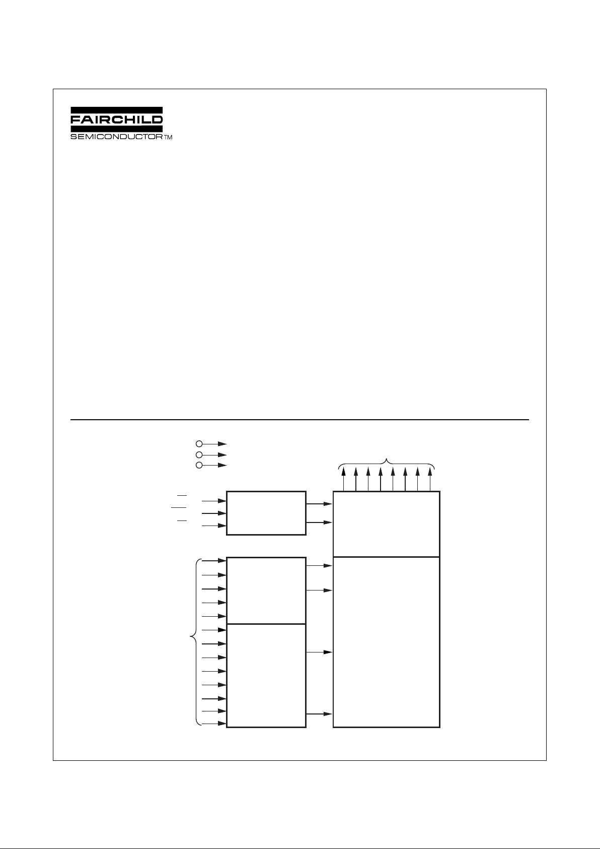
Block Diagram
January 1999
suited for high volume production applications where cost is an
important factor and programming only needs to be done once.
This family of EPROMs are fabricated with Fairchild’s proprietary,
time proven CMOS double-poly silicon gate technology which
combines high performance and high density with low power
consumption and excellent reliability.
Features
■ High performance CMOS
—150 ns access time
■ JEDEC standard pin configuration
—28-pin Plastic DIP package
—28-pin CERDIP package
■ Drop-in replacement for 27C64 or 2764
■ Manufacturers identification code
DS008634-1
Output Enable,
Chip Enable, and
Program Logic
Y Decoder
X Decoder
. . . . . . . . .
Output
Buffers
65,536-Bit
Cell Matrix
Data Outputs O0 - O
7
V
CC
GND
V
PP
OE
PGM
CE
A0 - A
12
Address
Inputs
© 1998 Fairchild Semiconductor Corporation
2
www.fairchildsemi.com
NMC27C64 Rev. C
NMC27C64 65,536-Bit (8192 x 8) CMOS EPROM
Connection Diagram
Note: Socket compatible EPROM pin configurations are shown in the blocks adjacent to the NMC27C64 pins.
V
CC
PGM
NC
A
8
A
9
A
11
OE
A
10
CE
O
7
O
6
O
5
O
4
O
3
1
2
3
4
5
6
7
8
9
10
11
12
13
14
28
27
26
25
24
23
22
21
20
19
18
17
16
15
V
PP
A
12
A
7
A
6
A
5
A
4
A
3
A
2
A
1
A
0
O
0
O
1
O
2
GND
A
15
A
12
A
7
A
6
A
5
A
4
A
3
A
2
A
1
A
0
O
0
O
1
O
2
GND
27C512
27512
27C256
27256
V
PP
A
12
A
7
A
6
A
5
A
4
A
3
A
2
A
1
A
0
O
0
O
1
O
2
GND
NMC27C64
A
7
A
6
A
5
A
4
A
3
A
2
A
1
A
0
O
0
O
1
O
2
GND
27C32
2732
A
7
A
6
A
5
A
4
A
3
A
2
A
1
A
0
O
0
O
1
O
2
GND
27C16
2716
V
PP
A
12
A
7
A
6
A
5
A
4
A
3
A
2
A
1
A
0
O
0
O
1
O
2
GND
27C128
27128
27C256
27256
27C512
27512
V
CC
A
14
A
13
A
8
A
9
A
11
OE
A
10
CE/PGM
O
7
O
6
O
5
O
4
O
3
V
CC
A
14
A
13
A
8
A
9
A
11
OE/V
PP
A
10
CE
O
7
O
6
O
5
O
4
O
3
V
CC
PGM
A
13
A
8
A
9
A
11
OE
A
10
CE
O
7
O
6
O
5
O
4
O
3
V
CC
A
8
A
9
V
PP
OE
A
10
CE/PGM
O
7
O
6
O
5
O
4
O
3
V
CC
A
8
A
9
A
11
OE/V
PP
A
10
CE
O
7
O
6
O
5
O
4
O
3
27C16
2716
27C32
2732
27C128
27128
DS008634-2
Pin Names
A0–A12 Addresses
CE Chip Enable
OE Output Enable
O0 –O
7
Outputs
PGM Program
NC No Connect
V
PP
Programming
Voltage
V
CC
Power Supply
GND Ground
Commercial Temperature Range V
CC
= 5V ±10%
Parameter/Order Number Access Time (ns)
NMC27C64Q, N 150 150
NMC27C64Q, N 200 200
Extended Temp Range (-40°C to +85°C) V
CC
= 5V ±10%
Parameter/Order Number Access Time (ns)
NMC27C64QE, NE200 200
3
www.fairchildsemi.com
NMC27C64 Rev. C
NMC27C64 65,536-Bit (8192 x 8) CMOS EPROM
READ OPERATION
DC Electrical Characteristics
Symbol Parameter Conditions Min Typ Max Units
I
LI
Input Load Current VIN = VCC or GND 10 µA
I
LO
Output Leakage Current V
OUT
= VCC or GND, CE = V
IH
10 µA
I
CC1
V
CC
Current (Active) CE = VIL ,f=5 MHz 5 20 mA
(Note 9) TTL Inputs Inputs = VIH or VIL, I/O = 0 mA
I
CC2
VCC Current (Active) CE = GND, f = 5 MHz 3 10 mA
(Note 9) CMOS Inputs Inputs = VCC or GND, I/O = 0 mA
I
CCSB1
V
CC
Current (Standby) CE = V
IH
0.1 1 mA
TTL Inputs
I
CCSB2
VCC Current (Standby) CE = V
CC
0.5 100 µA
CMOS Inputs
I
PP
VPP Load Current VPP = V
CC
10 µA
V
IL
Input Low Voltage -0.1 0.8 V
V
IH
Input High Voltage 2.0 VCC +1 V
V
OL1
Output Low Voltage IOL = 2.1 mA 0.45 V
V
OH1
Output High Voltage IOH = -400 µA 2.4 V
V
OL2
Output Low Voltage IOL = 0 µA 0.1 V
V
OH2
Output High Voltage IOH = 0 µAV
CC
- 0.1 V
AC Electrical Characteristics
NMC27C64
Symbol Parameter Conditions 150 200, E200 Units
Min Max Min Max
t
ACC
Address to CE = OE = V
IL
150 200 ns
Output Delay PGM = V
IH
t
CE
CE to Output Delay
OE = VIL, PGM = V
IH
150 200 ns
t
OE
OE to Output Delay
CE = VIL, PGM = V
IH
60 60 ns
t
DF
OE High to Output Float CE = VIL, PGM = V
IH
0 60 0 60 ns
t
CF
CE High to Output Float OE = VIL, PGM = V
IH
0 60 0 60 ns
t
OH
Output Hold from CE = OE = V
IL
Addresses, CE or OE , PGM = V
IH
00ns
Whichever Occurred First
Absolute Maximum Ratings (Note 1)
Temperature Under Bias -55°C to +125°C
Storage Temperature -65°C to +150°C
All Input Voltages except A9
with Respect to Ground (Note 10) +6.5V to -0.6V
All Output Voltages
with Respect to Ground (Note 10)VCC +1.0V to GND -0.6V
VPP Supply Voltage and A
9
with Respect to Ground
During Programming +14.0V to -0.6V
VCC Supply Voltage with
Respect to Ground +7.0V to -0.6V
Power Dissipation 1.0W
Lead Temperature
(Soldering, 10 sec.) 300°C
ESD Rating
(Mil Spec 883C,
Method 3015.2) 2000V
Operating Conditions (Note 7)
Temperature Range
NMC27C64Q 150, 200 0°C to +70°C
NMC27C64N 150, 200
NMC27C64QE 200 -40°C to +85°C
NMC27C64NE 200
VCC Power Supply +5V ±10%
 Loading...