

Fairchild Semiconductor NMC27C32BQ150, NMC27C32BQ200 Datasheet
TL/D/8827
NMC27C32B 32,768-Bit (4096 x 8) CMOS EPROM
December 1996
NMC27C32B
32,768-Bit (4096 x 8) CMOS EPROM
General Description
The NMC27C32B is a 32k UV erasable and electrically reprogrammable CMOS EPROM, ideally suited for applications where fast turnaround, pattern experimentation and
low power consumption are important requirements.
The NMC27C32B is designed to operate with a single
a
5V
power supply with
g
10% tolerance.
The NMC27C32B is packaged in a 24-pin dual-in-line package with a quartz window. The quartz window allows the
user to expose the chip to ultraviolet light to erase the bit
pattern. A new pattern can then be written electrically into
the device by following the programming procedure.
This EPROM is fabricated with National’s proprietary, time
proven CMOS double-poly silicon gate technology which
combines high performance and high density with low power consumption and excellent reliability.
Features
Y
Low CMOS power consumption
Ð Active Power: 55 mW Max
Ð Standby Power: 0.55 mW Max
Y
Extended temperature range,b40§Ctoa85§C
Y
Fast and reliable programming
Y
TTL, CMOS compatible inputs/outputs
Y
TRI-STATEÉoutput
Y
Manufacturer’s identification code for automatic
programming
Y
High current CMOS level output drivers
Y
Compatible with NMOS 2732
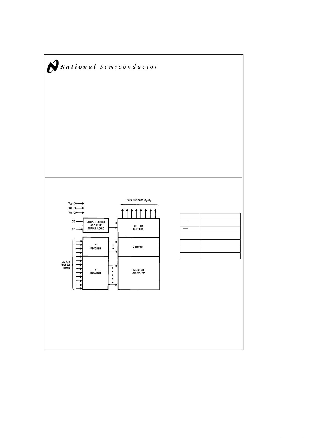
Block Diagram
TL/D/8827– 1
Pin Names
A0–A11 Addresses
CE Chip Enable
OE Output Enable
V
PP
Programming Voltage
O0–O7Outputs
V
CC
Power Supply
GND Ground
TRI-STATEÉis a registered trademark of National Semiconductor Corporation.
C
1996 National Semiconductor Corporation RRD-B30M17/Printed in U. S. A.
http://www.national.com
Connection Diagram
27C256 27C128 27C64 27C16
27256 27128 2764 2716
V
PP
V
PP
V
PP
A12 A12 A12
A7 A7 A7 A7
A6 A6 A6 A6
A5 A5 A5 A5
A4 A4 A4 A4
A3 A3 A3 A3
A2 A2 A2 A2
A1 A1 A1 A1
A0 A0 A0 A0
O
0
O
0
O
0
O
0
O
1
O
1
O
1
O
1
O
2
O
2
O
2
O
2
GND GND GND GND
NMC27C32B
Dual-In-Line Package
TL/D/8827– 2
27C16 27C64 27C128 27C256
2716 2764 27128 27256
V
CC
V
CC
V
CC
PGM PGM A14
V
CC
NC A13 A13
A8 A8 A8 A8
A9 A9 A9 A9
V
PP
A11 A11 A11
OE
OE OE OE
A10 A10 A10 A10
CE
CE CE CE
O
7
O
7
O
7
O
7
O
6
O
6
O
6
O
6
O
5
O
5
O
5
O
5
O
4
O
4
O
4
O
4
O
3
O
3
O
3
O
3
Note: Socket compatible EPROM pin configurations are shown in the blocks adjacent to the NMC27C32B pins.
Order Number NMC27C32BQ
See NS Package Number J24AQ
Commercial Temp Range (0
§
Ctoa70§C) V
CC
e
5Vg10%
Parameter/Order Number Access Time (ns)
NMC27C32BQ150 150
NMC27C32BQ200 200
NMC27C32BQ250 250
Extended Temp Range (b40§Ctoa85§C) V
CC
e
5Vg10%
Parameter/Order Number Access Time (ns)
NMC27C32BQE200 200
http://www.national.com 2
Absolute Maximum Ratings (Note 1)
If Military/Aerospace specified devices are required,
please contact the National Semiconductor Sales
Office/Distributors for availability and specifications.
Temperature Under Bias
b
40§Ctoa85§C
Storage Temperature
b
65§Ctoa150§C
V
CC
Supply Voltage with
Respect to Ground
a
7.0V tob0.6V
All Input Voltages except A9
and OE
/VPPwith
Respect to Ground (Note 9)
a
6.5V tob0.6V
All Output Voltages with
Respect to Ground (Note 9) V
CC
a
1.0V to GNDb0.6V
OE
/VPPSupply and A9 Voltage with
Respect to Ground
a
14.0V tob0.6V
Power Dissipation 1.0W
Lead Temperature (Soldering, 10 sec.) 300
§
C
Operating Conditions (Note 6)
Temperature Range
NMC27C32BQ150, 200, 250 0
§
Ctoa70§C
NMC27C32BQE200
b
40§Ctoa85§C
VCCPower Supply
a
5Vg10%
READ OPERATION
DC Electrical Characteristics
Symbol Parameter Conditions Min Typ Max Units
I
LI
Input Load Current V
IN
e
VCCor GND 0.01 1 mA
I
PP
OE/VPPLoad Current OE/V
PP
e
VCCor GND 10 mA
I
LO
Output Leakage Current V
OUT
e
VCCor GND, CEeV
IH
0.01 1 mA
I
CC1
VCCCurrent (Active) CEeVIL,fe5 MHz
520mA
TTL Inputs Inputs
e
VIHor VIL, I/Oe0mA
I
CC2
VCCCurrent (Active) CEeGND, fe5 MHz
310mA
CMOS Inputs Inputs
e
VCCor GND, I/Oe0mA
I
CCSB1
VCCCurrent (Standby) CEeV
IH
0.1 1 mA
TTL Inputs
I
CCSB2
VCCCurrent (Standby) CEeV
CC
0.5 100 mA
CMOS Inputs
V
IL
Input Low Voltage
b
0.2 0.8 V
V
IH
Input High Voltage 2.0 V
CC
a
1V
V
OL1
Output Low Voltage I
OL
e
2.1 mA 0.45 V
V
OH1
Output High Voltage I
OH
eb
400 mA 2.4 V
V
OL2
Output Low Voltage I
OL
e
10 mA 0.1 V
V
OH2
Output High Voltage I
OH
eb
10 mAV
CC
b
0.1 V
AC Electrical Characteristics
NMC27C32B
Symbol Parameter Conditions Q150 Q200, QE200 Q250 Units
Min Max Min Max Min Max
t
ACC
Address to Output Delay CEeOEeV
IL
150 200 250 ns
t
CE
CE to Output Delay OEeV
IL
150 200 250 ns
t
OE
OE to Output Delay CEeV
IL
60 60 70 ns
t
DF
OE High to Output Float CEeV
IL
0 50 0 60 0 70 ns
t
CF
CE High to Output Float OEeV
IL
0 50 0 60 0 60 ns
t
OH
Output Hold from Addresses, CEeOEeV
IL
CE or OE, Whichever 0 0 0 ns
Occurred First
http://www.national.com3
 Loading...