

Fairchild Semiconductor NM93CS06M8X, NM93CS06M8, NM93CS06LZM8X, NM93CS06LZM8, NM93CS06LM8X Datasheet
...
1
www.fairchildsemi.com
NM93CS06 Rev. F.2
NM93CS06 (MICROWIRE Bus Interface) 256-Bit Serial EEPROM
with Data Protect and Sequential Read
February 2000
© 1999 Fairchild Semiconductor Corporation
NM93CS06
(MICROWIRE™ Bus Interface) 256-Bit Serial EEPROM
with Data Protect and Sequential Read
General Description
NM93CS06 is a 256-bit CMOS non-volatile EEPROM organized
as 16 x 16-bit array. This device features MICROWIRE interface
which is a 4-wire serial bus with chipselect (CS), clock (SK), data
input (DI) and data output (DO) signals. This interface is compatible to many of standard Microcontrollers and Microprocessors.
NM93CS06 offers programmable write protection to the memory
array using a special register called Protect Register. Selected
memory locations can be protected against write by programming
this Protect Register with the address of the first memory location
to be protected (all locations greater than or equal to this first
address are then protected from further change). Additionally, this
address can be “permanently locked” into the device, making all
future attempts to change data impossible. In addition this device
features “sequential read”, by which, entire memory can be read
in one cycle instead of multiple single byte read cycles. There are
10 instructions implemented on the NM93CS06, 5 of which are for
memory operations and the remaining 5 are for Protect Register
operations. This device is fabricated using Fairchild Semiconductor floating-gate CMOS process for high reliability, high endurance
and low power consumption.
“LZ” and “L” versions of NM93CS06 offer very low standby current
making them suitable for low power applications. This device is offered
in both SO and TSSOP packages for small space considerations.
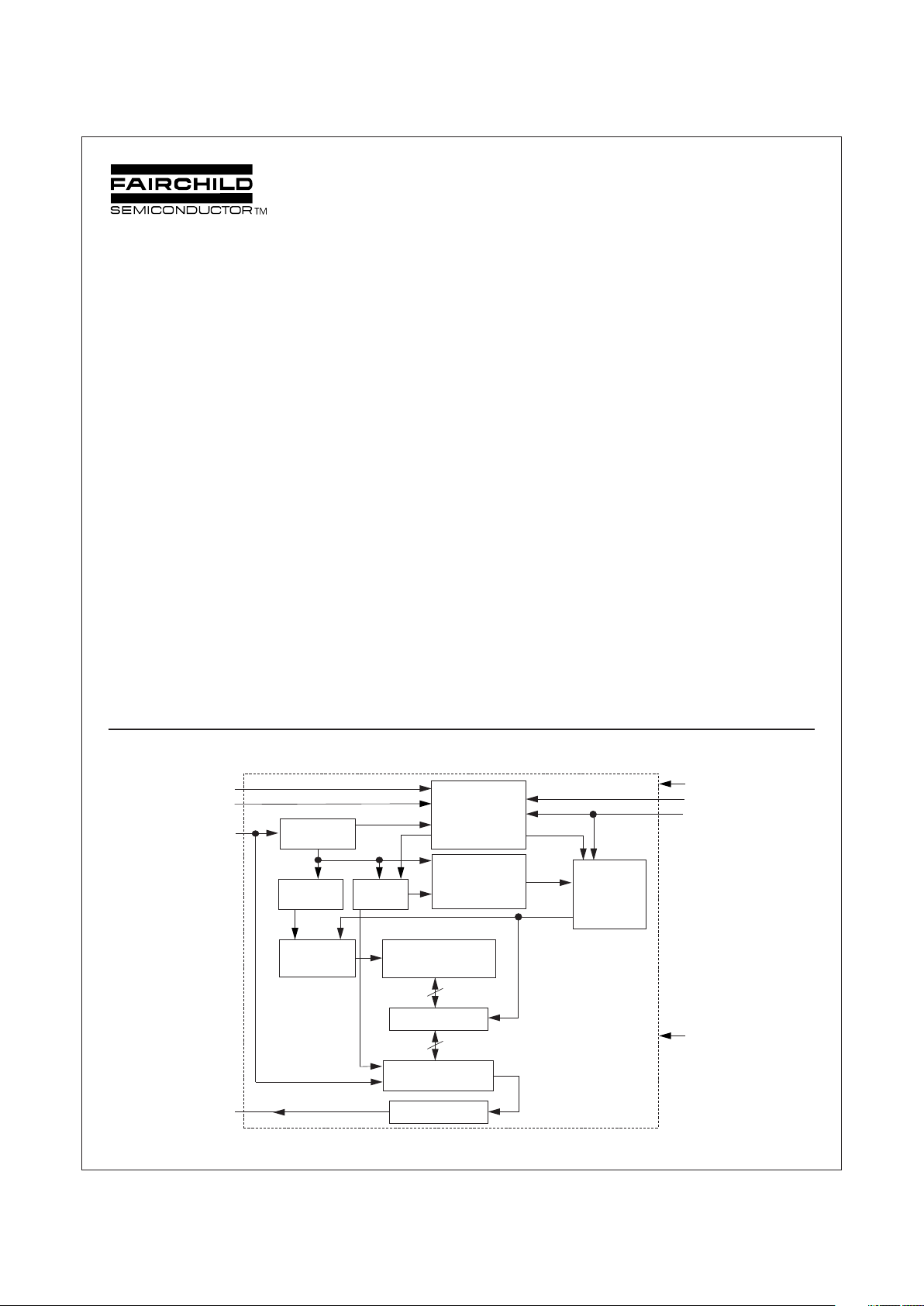
Functional Diagram
Features
■ Wide VCC 2.7V - 5.5V
■ Programmable write protection
■ Sequential register read
■ Typical active current of 200µA
10µA standby current typical
1µA standby current typical (L)
0.1µA standby current typical (LZ)
■ No Erase instruction required before Write instruction
■ Self timed write cycle
■ Device status during programming cycles
■ 40 year data retention
■ Endurance: 1,000,000 data changes
■ Packages available: 8-pin SO, 8-pin DIP, 8-pin TSSOP
INSTRUCTION
DECODER
CONTROL LOGIC
AND CLOCK
GENERATORS
COMPARATOR
AND
WRITE ENABLE
HIGH VOLTAGE
GENERATOR
AND
PROGRAM
TIMER
INSTRUCTION
REGISTER
ADDRESS
REGISTER
PROTECT
REGISTER
EEPROM ARRAY
READ/WRITE AMPS
DATA IN/OUT REGISTER
16 BITS
DECODER
16
16
DATA OUT BUFFER
PRE
PE
CS
SK
DI
DO
V
SS
V
CC
2
www.fairchildsemi.com
NM93CS06 Rev. F.2
NM93CS06 (MICROWIRE Bus Interface) 256-Bit Serial EEPROM
with Data Protect and Sequential Read
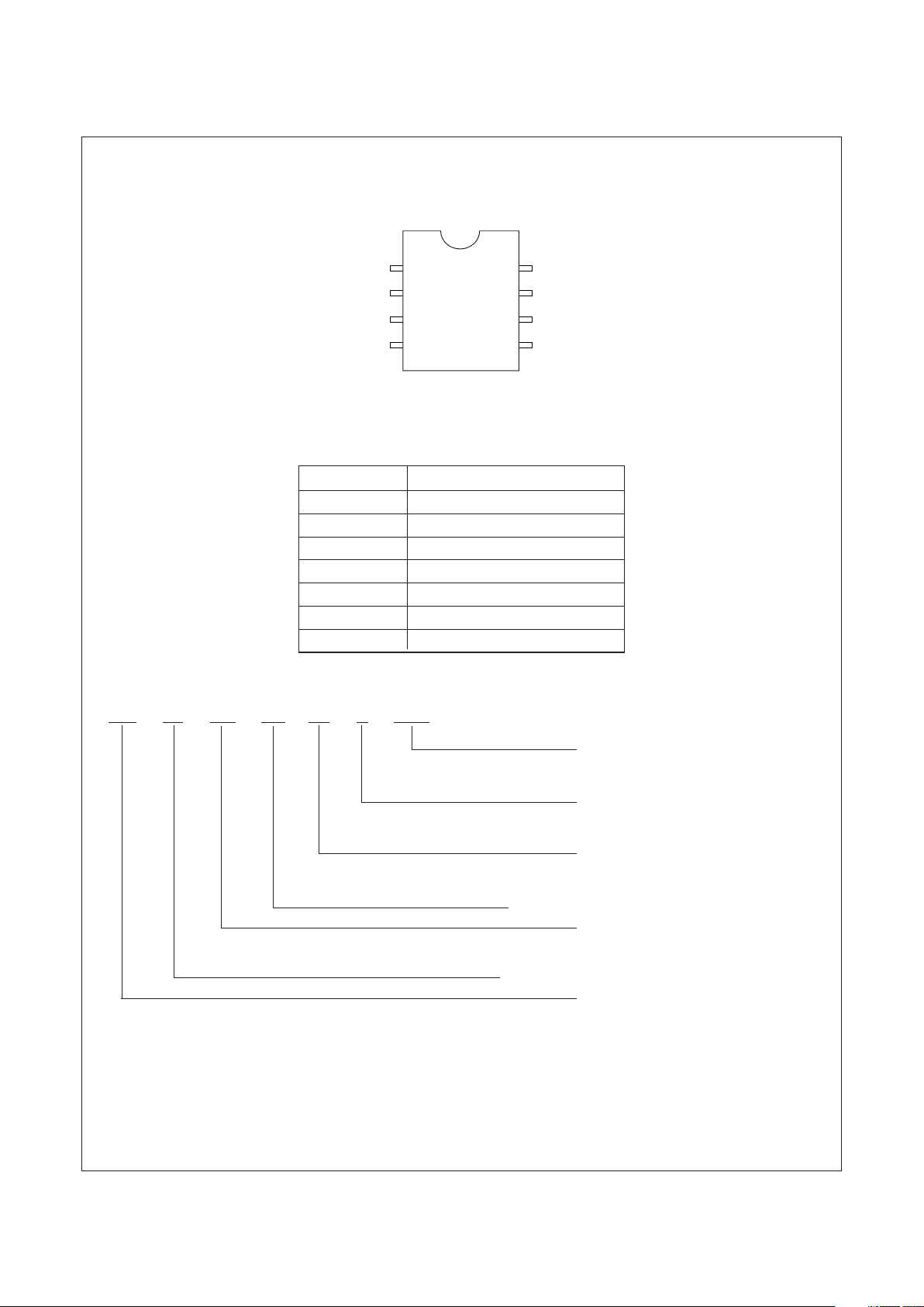
Connection Diagram
Dual-In-Line Package (N)
8–Pin SO (M8) and 8–Pin TSSOP (MT8)
Top View
Package Number
N08E, M08A and MTC08
Pin Names
CS Chip Select
SK Serial Data Clock
DI Serial Data Input
DO Serial Data Output
GND Ground
PE Program Enable
PRE Protect Register Enable
V
CC
Power Supply
Ordering Information
NM 93 CS XX LZ E XXX Letter Description
Package N 8-pin DIP
M8 8-pin SO
MT8 8-pin TSSOP
Temp. Range None 0 to 70°C
V -40 to +125°C
E -40 to +85°C
Voltage Operating Range Blank 4.5V to 5.5V
L 2.7V to 5.5V
LZ 2.7V to 5.5V and
<1µA Standby Current
Density 06 256 bits
C CMOS
CS Data protect and sequential
read
Interface 93 MICROWIRE
Fairchild Memory Prefix
V
CC
PE
GND
CS
SK
DI
DO
1
2
3
4
8
7
6
5
PRE
3
www.fairchildsemi.com
NM93CS06 Rev. F.2
NM93CS06 (MICROWIRE Bus Interface) 256-Bit Serial EEPROM
with Data Protect and Sequential Read
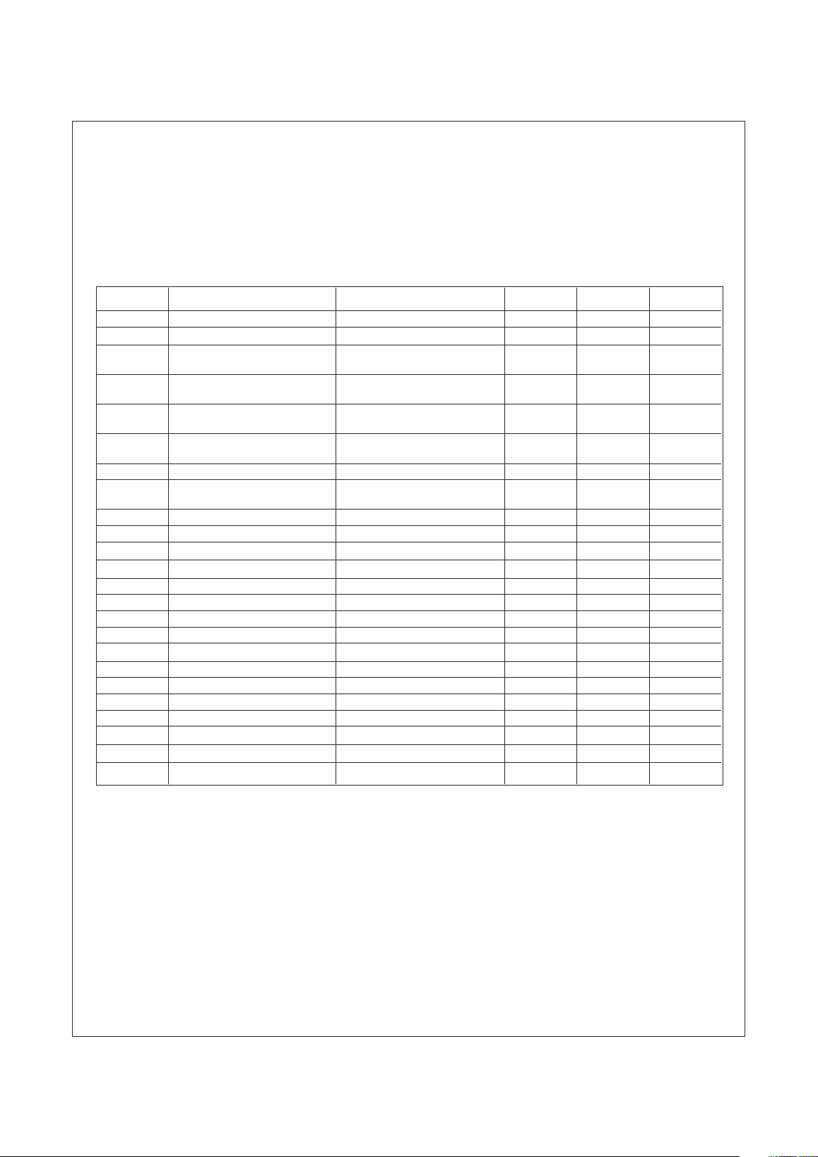
Absolute Maximum Ratings (Note 1)
Ambient Storage Temperature -65°C to +150°C
All Input or Output Voltages +6.5V to -0.3V
with Respect to Ground
Lead Temperature
(Soldering, 10 sec.) +300°C
ESD rating 2000V
Operating Conditions
Ambient Operating Temperature
NM93CS06 0°C to +70°C
NM93CS06E -40°C to +85°C
NM93CS06V -40°C to +125°C
Power Supply (V
CC
) 4.5V to 5.5V
DC and AC Electrical Characteristics V
CC
= 4.5V to 5.5V unless otherwise specified
Symbol Parameter Conditions Min Max Units
I
CCA
Operating Current CS = VIH, SK=1.0 MHz 1 mA
I
CCS
Standby Current CS = V
IL
50 µA
I
IL
Input Leakage VIN = 0V to V
CC
±-1 µA
I
OL
Output Leakage (Note 2)
V
IL
Input Low Voltage -0.1 0.8 V
V
IH
Input High Voltage 2 VCC +1
V
OL1
Output Low Voltage IOL = 2.1 mA 0.4 V
V
OH1
Output High Voltage IOH = -400 µA 2.4
V
OL2
Output Low Voltage IOL = 10 µA 0.2 V
V
OH2
Output High Voltage IOH = -10 µAV
CC
- 0.2
f
SK
SK Clock Frequency (Note 3) 1 MHz
t
SKH
SK High Time 0°C to +70°C 250 ns
-40°C to +125°C 300
t
SKL
SK Low Time 250 ns
t
SKS
SK Setup Time 50 ns
t
CS
Minimum CS Low Time (Note 4) 250 ns
t
CSS
CS Setup Time 100 ns
t
PRES
PRE Setup Time 50 ns
t
DH
DO Hold Time 70 ns
t
PES
PE Setup Time 50 ns
t
DIS
DI Setup Time 100 ns
t
CSH
CS Hold Time 0 ns
t
PEH
PE Hold Time 250 ns
t
PREH
PRE Hold Time 50 ns
t
DIH
DI Hold Time 20 ns
t
PD
Output Delay 500 ns
t
SV
CS to Status Valid 500 ns
t
DF
CS to DO in Hi-Z CS = V
IL
100 ns
t
WP
Write Cycle Time 10 ms
4
www.fairchildsemi.com
NM93CS06 Rev. F.2
NM93CS06 (MICROWIRE Bus Interface) 256-Bit Serial EEPROM
with Data Protect and Sequential Read
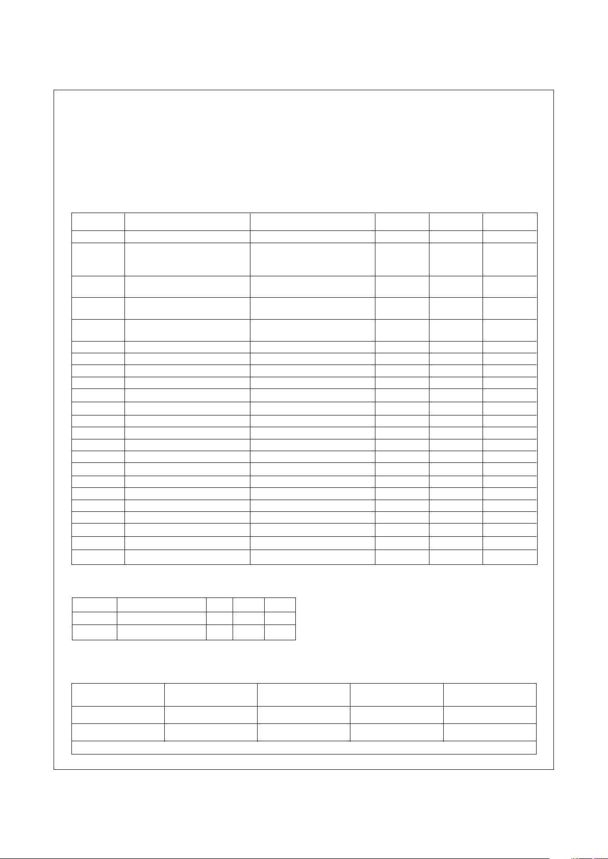
Absolute Maximum Ratings (Note 1)
Ambient Storage Temperature -65°C to +150°C
All Input or Output Voltages +6.5V to -0.3V
with Respect to Ground
Lead Temperature
(Soldering, 10 sec.) +300°C
ESD rating 2000V
Operating Conditions
Ambient Operating Temperature
NM93CS06L/LZ 0°C to +70°C
NM93CS06LE/LZE -40°C to +85°C
NM93CS06LV/LZV -40°C to +125°C
Power Supply (V
CC
) 2.7V to 5.5V
DC and AC Electrical Characteristics V
CC
= 2.7V to 5.5V unless otherwise specified
Symbol Parameter Conditions Min Max Units
I
CCA
Operating Current CS = VIH, SK=1.0 MHz 1 mA
I
CCS
Standby Current CS = V
IL
L 10 µA
LZ (2.7V to 4.5V) 1 µA
I
IL
Input Leakage VIN = 0V to V
CC
±1 µA
I
OL
Output Leakage (Note 2)
V
IL
Input Low Voltage -0.1 0.15V
CC
V
V
IH
Input High Voltage 0.8V
CC
VCC +1
V
OL
Output Low Voltage IOL = 10µA 0.1V
CC
V
V
OH
Output High Voltage IOH = -10µA 0.9V
CC
f
SK
SK Clock Frequency (Note 3) 0 250 KHz
t
SKH
SK High Time 1 µs
t
SKL
SK Low Time 1 µs
t
SKS
SK Setup Time 0.2 µs
t
CS
Minimum CS Low Time (Note 4) 1 µs
t
CSS
CS Setup Time 0.2 µs
t
PRES
PRE Setup Time 50 ns
t
DH
DO Hold Time 70 ns
t
PES
PE Setup Time 50 ns
t
DIS
DI Setup Time 0.4 µs
t
CSH
CS Hold Time 0 ns
t
PEH
PE Hold Time 250 ns
t
PREH
PRE Hold Time 50 ns
t
DIH
DI Hold Time 0.4 µs
t
PD
Output Delay 2 µs
t
SV
CS to Status Valid 1 µs
t
DF
CS to DO in Hi-Z CS = V
IL
0.4 µs
t
WP
Write Cycle Time 15 ms
Capacitance TA = 25°C, f = 1 MHz (Note 5)
Symbol Test Typ Max Units
C
OUT
Output Capacitance 5 pF
C
IN
Input Capacitance 5 pF
Note 1: Stress above those listed under “Absolute Maximum Ratings” may cause permanent damage
to the device. This is a stress rating only and functional operation of the device at these or any other
conditions above those indicated in the operational sections of the specification is not implied. Exposure
to absolute maximum rating conditions for extended periods may affect device reliability.
Note 2: Typical leakage values are in the 20nA range.
Note 3: The shortest allowable SK clock period = 1/f
SK
(as shown under the fSK parameter). Maximum
SK clock speed (minimum SK period) is determined by the interaction of several AC parameters stated
in the datasheet. Within this SK period, both t
SKH
and t
SKL
limits must be observed. Therefore, it is not
allowable to set 1/fSK = t
SKHminimum
+ t
SKLminimum
for shorter SK cycle time operation.
Note 4: CS (Chip Select) must be brought low (to V
IL
) for an interval of tCS in order to reset all internal
device registers (device reset) prior to beginning another opcode cycle. (This is shown in the opcode
diagram on the following page.)
Note 5: This parameter is periodically sampled and not 100% tested.
AC Test Conditions
VCC Range VIL/V
IH
VIL/V
IH
VOL/V
OH
IOL/I
OH
Input Levels Timing Level Timing Level
2.7V ≤ VCC ≤ 5.5V 0.3V/1.8V 1.0V 0.8V/1.5V ±10µA
(Extended Voltage Levels)
4.5V ≤ VCC ≤ 5.5V 0.4V/2.4V 1.0V/2.0V 0.4V/2.4V 2.1mA/-0.4mA
(TTL Levels)
Output Load: 1 TTL Gate (CL = 100 pF)
5
www.fairchildsemi.com
NM93CS06 Rev. F.2
NM93CS06 (MICROWIRE Bus Interface) 256-Bit Serial EEPROM
with Data Protect and Sequential Read
Pin Description
Chip Select (CS)
This is an active high input pin to NM93CS06 EEPROM (the device)
and is generated by a master that is controlling the device. A high
level on this pin selects the device and a low level deselects the
device. All serial communications with the device is enabled only
when this pin is held high. However this pin cannot be permanently
tied high, as a rising edge on this signal is required to reset the
internal state-machine to accept a new cycle and a falling edge to
initiate an internal programming after a write cycle. All activity on the
SK, DI and DO pins are ignored while CS is held low.
Serial Clock (SK)
This is an input pin to the device and is generated by the master that
is controlling the device. This is a clock signal that synchronizes the
communication between a master and the device. All input information (DI) to the device is latched on the rising edge of this clock input,
while output data (DO) from the device is driven from the rising edge
of this clock input. This pin is gated by CS signal.
Serial Input (DI)
This is an input pin to the device and is generated by the master
that is controlling the device. The master transfers Input information (Start bit, Opcode bits, Array addresses and Data) serially via
this pin into the device. This Input information is latched on the
rising edge of the SCK. This pin is gated by CS signal.
Serial Output (DO)
This is an output pin from the device and is used to transfer Output
data via this pin to the controlling master. Output data is serially
shifted out on this pin from the rising edge of the SCK. This pin is
active only when the device is selected.
Protect Register Enable (PRE)
This is an active high input pin to the device and is used to
distinguish operations to memory array and operations to Protect
Register. When this pin is held low, operations to the memory
array are enabled. When this pin is held high, operations to the
Protect Register are enabled. This pin operates in conjunction
with PE pin. Refer Table1 for functional matrix of this pin for
various operations.
Program Enable (PE)
This is an active high input pin to the device and is used to enable
operations, that are write in nature, to the memory array and to the
Protect register. When this pin is held high, operations that are
“write” in nature are enabled. When this pin is held low, operations
that are “write” in nature are disabled. This pin operates in
conjunction with PRE pin. Refer Table1 for functional matrix of this
pin for various operations.
Microwire Interface
A typical communication on the Microwire bus is made through the
CS, SK, DI and DO signals. To facilitate various operations on the
Memory array and on the Protect Register, a set of 10 instructions
are implemented on NM93CS06. The format of each instruction is
listed in Table 1.
Instruction
Each of the above 10 instructions is explained under individual
instruction descriptions.
Start Bit
This is a 1-bit field and is the first bit that is clocked into the device
when a Microwire cycle starts. This bit has to be “1” for a valid cycle
to begin. Any number of preceding “0” can be clocked into the
device before clocking a “1”.
Opcode
This is a 2-bit field and should immediately follow the start bit.
These two bits (along with PRE, PE signals and 2 MSB of address
field) select a particular instruction to be executed.
Address Field
This is a 6-bit field and should immediately follow the Opcode bits.
In NM93CS06, only the LSB 4 bits are used for address decoding
during READ, WRITE and PRWRITE instructions. During these
instructions (READ, WRITE and PRWRITE), the MSB 2 bits are
"don't care" (can be 0 or 1). During all other instructions (with the
exception of PRREAD), the MSB 2 bits are used to decode
instruction (along with Opcode bits, PRE and PE signals).
Data Field
This is a 16-bit field and should immediately follow the Address
bits. Only the WRITE and WRALL instructions require this field.
D15 (MSB) is clocked first and D0 (LSB) is clocked last (both
during writes as well as reads).
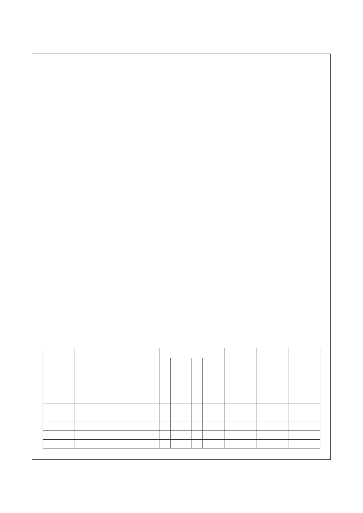
TABLE 1. Instruction set
Instruction Start Bit Opcode Field Address Field Data Field PRE Pin PE Pin
READ 1 10 X X A3 A2 A1 A0 0 X
WEN 1 00 1 1XXXX 0 1
WRITE 1 01 X X A3 A2 A1 A0 D15-D0 0 1
WRALL 1 00 0 1 XXXX D15-D0 0 1
WDS 1 00 0 0XXXX 0 X
PRREAD 1 10 X X XXXX 1 X
PREN 1 00 1 1 XXXX 1 1
PRCLEAR 1 11 111111 1 1
PRWRITE 1 01 X X A3 A2 A1 A0 1 1
PRDS 1 00 000000 1 1
 Loading...