

Fairchild Semiconductor NM27LV210V250, NM27LV210V200 Datasheet
1
www.fairchildsemi.com
NM27LV210 1,048,576-Bit (64K x 16) Low Voltage EPROM
NM27LV210
1,048,576-Bit (64K x 16) Low Voltage EPROM
General Description
The NM27LV210 is a high performance Low Voltage Electrical
Programmable read only memory. It is manufactured using
Fairchild’s latest EPROM technology. This technology allows the
part to operate at high speeds.
This Low Voltage and Low Power EPROM is designed with power
sensitive hand held and portable battery products in mind. This
allows for code storage of firmware for applications like notebook
computers, palm top computers, cellular phones, and HDD.
The NM27LV210 is one member of Fairchild’s growing Low
Voltage product family.
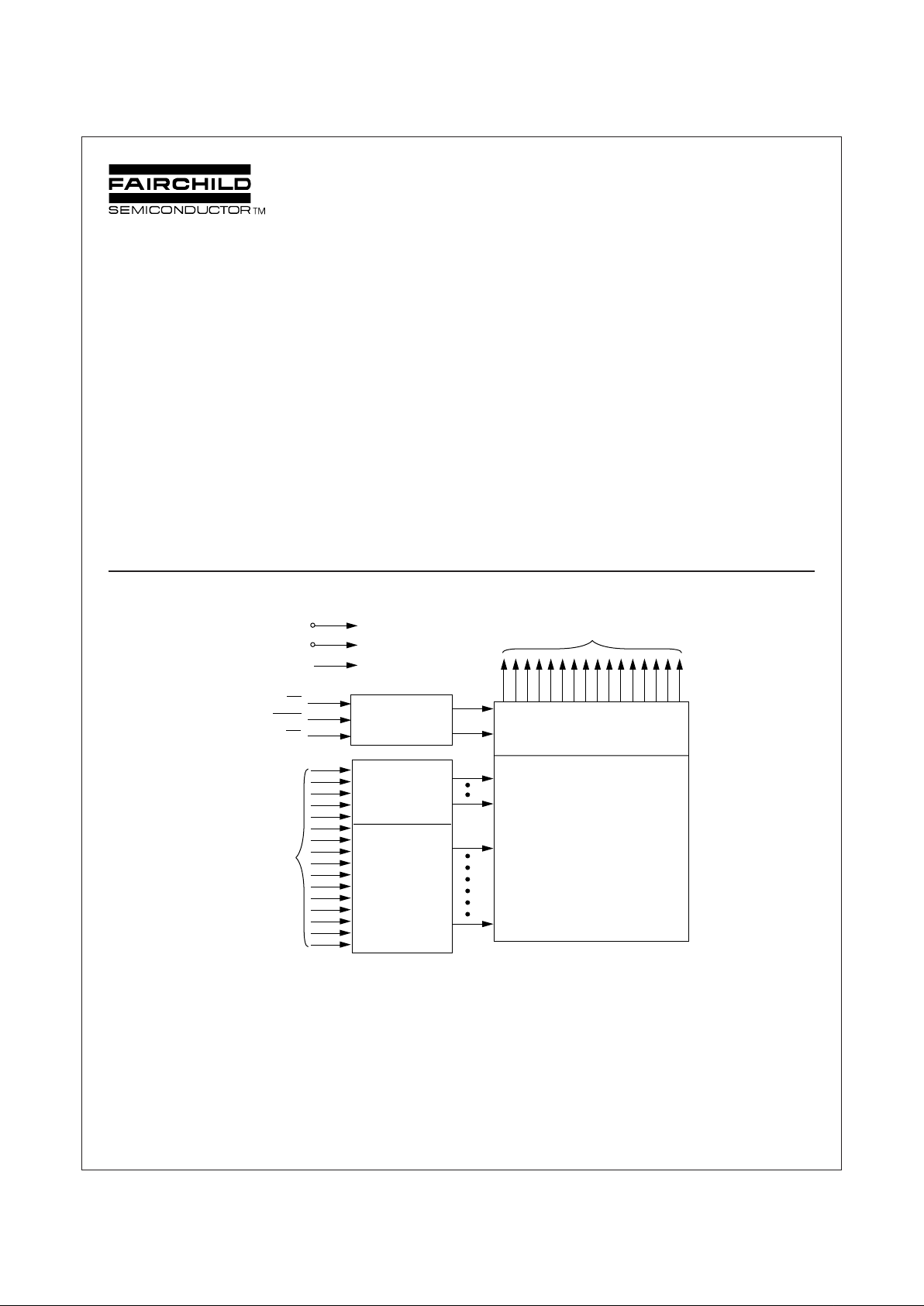
Block Diagram
July 1998
Features
■ 3.0V to 3.6V operation
■ 200 ns, 250 ns maximum access time
■ Low current operation
—20mA ICC active current @ 5 MHz
—50µA I
CC
standby current @ 5 MHz
■ Ultra low power operation
—60 µA standby power @ 3.3V
—50 mW active power @ 3.3V
■ Surface mount package option
—44-Pin PLCC
DS011376-1
© 1998 Fairchild Semiconductor Corporation
V
cc
GND
V
pp
OE
PGM
Output Enable
Chip Enable, and
Program Logic
Y
Decoder
X
Decoder
Output
Buffers
1,048,576-Bit
Cell Matrix
A
0 - A15
Address
Inputs
Data Outputs O
0 - O15
CE
2
www.fairchildsemi.com
NM27LV210 1,048,576-Bit (64K x 16) Low Voltage EPROM
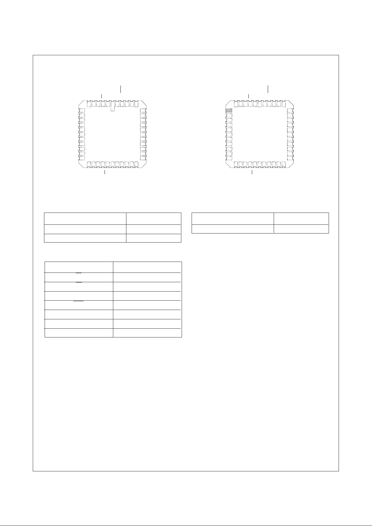
Connection Diagrams
PLCC Pin Configuration
Top View
Commercial Temperature Range
(0°C to +70°C) VCC = 3.3V ± 0.3
Parameter/Order Number Access Time (ns)
NM27LV210 V 200 200
NM27LV210 V 250 250
Pin Names
A0–A15 Addresses
CE Chip Enable
OE Output Enable
O0–O15 Outputs
PGM Program
XX Don’t Care (During Read)
NC No Connect
V
PP
Programming Voltage
Extended Temperature Range
(-40°C to +85°C) VCC = 3.3V ±0.3
Parameter/Order Number Access Time (ns)
NM27LV210 VE 250 250
• All packages conform to JEDEC standard.
• All versions are guaranteed to function in slower applications.
• Consult the FSC representative for newly released products/
packages.
O
12
O
11
O
10
O
9
O
8
GND
NC
O
7
O
6
O
5
O
4
A
13
A
12
A
11
A
10
A
9
GND
NC
A
8
A
7
A
6
A
5
O13O14O15XX/VPPNC
NC
A15A
14
O3O2O1O
0
OE
NC
A
0A1A2A3A4
1
23456
7
8
9
10
11
12
13
14
15
16
17
4041424344
38
37
36
35
34
33
32
31
30
2221201918 282726252423
29
39
CE
VCCXX/PGM
O
12
O
11
O
10
O
9
O
8
GND
NC
O
7
O
6
O
5
O
4
A
13
A
12
A
11
A
10
A
9
GND
NC
A
8
A
7
A
6
A
5
O13O14O15XX/VPPNC
NC
A15A
14
O3O2O1O
0
OE
NC
A
0A1A2A3A4
39
4041424344
1
2
3
4
5
6
7
8
9
10
11
3435363738
32
31
30
29
28
27
26
25
24
1615141312 222120191817
23
33
CE
VCCXX/PGM
DS011376-7
DS011376-3
3
www.fairchildsemi.com
NM27LV210 1,048,576-Bit (64K x 16) Low Voltage EPROM
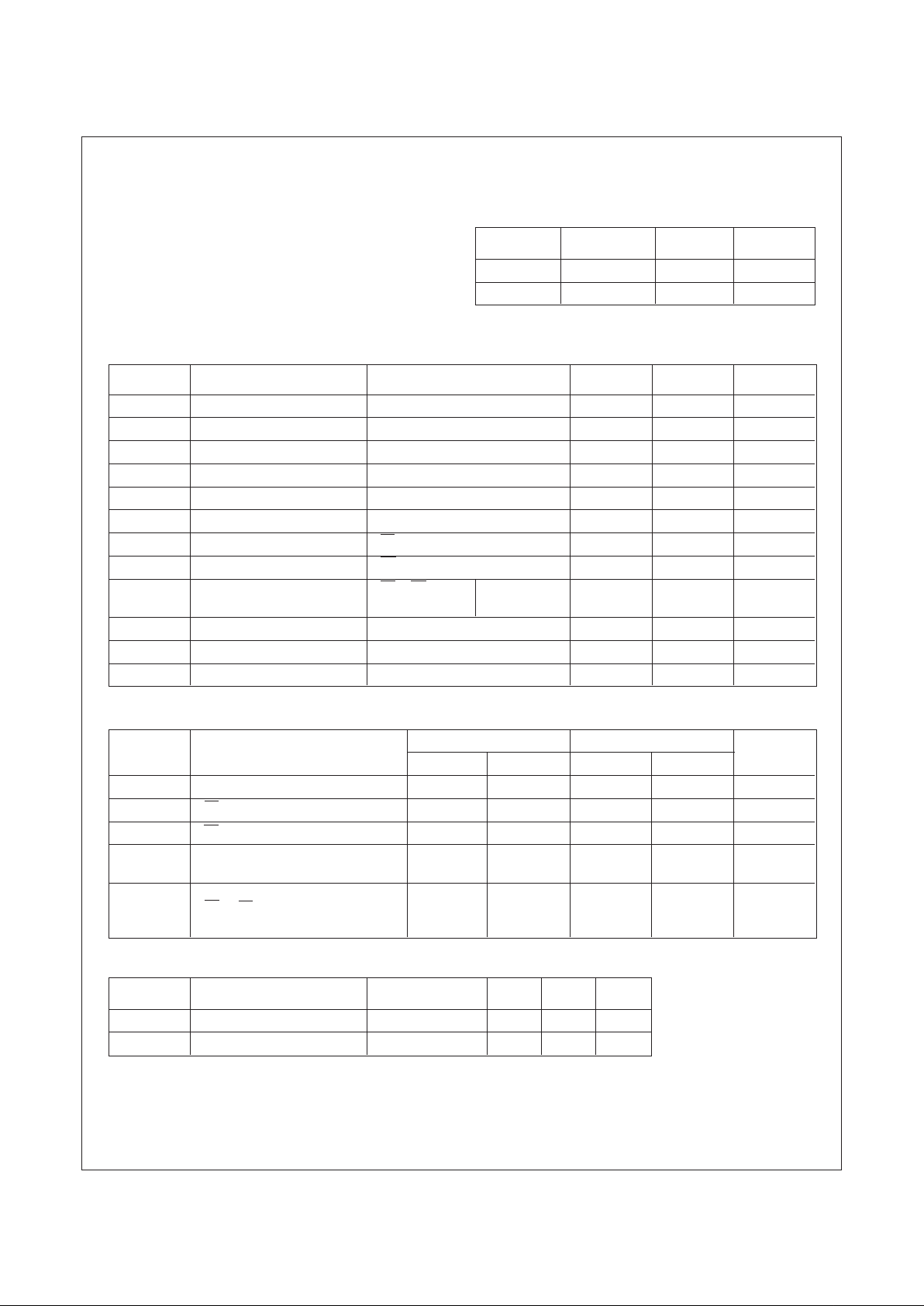
Absolute Maximum Ratings (Note 2)
Storage Temperature -65°C to +150°C
All Input Voltages except A9 with
Respect to Ground (Note 12) -0.6V to +7V
VPP and A9 with Respect to Ground -0.6V to +14V
VCC Supply Voltage with
Respect to Ground -0.6V to +7V
ESD Protection >2000V
All Output Voltages with
Respect to Ground (Note 11) VCC + 1.0V to GND - 0.6V
Operating Range
Range Temperature V
CC
Tolerance
Commercial 0°C to +70°C 3.3 ±0.3
Extended -40°C to +85°C 3.3 ±0.3
DC Read Characteristics Over Operating Range with V
PP
= V
CC
Symbol Parameter Test Conditions Min Max Units
V
IL
Input Low Level -0.3 0.7 V
V
IH
Input High Level 2.0 VCC + 0.3 V
V
OL1
Output Low Voltage (TTL) 0.4 V
V
OH1
Output High Voltage (TTL) 2.4 V
V
OL2
Output Low Voltage (CMOS) 0.2 V
V
OH2
Output High Voltage (CMOS) VCC - 0.3 V
I
SB1
VCC Standby Current (TTL) CE = V
IH
150 µA
I
SB2
VCC Standby Current (CMOS) CE = VCC ±0.3V 50 µA
I
CC
VCC Active Current CE = OE = VIL, f = 5 MHz 20 mA
I/O = 0 µA
I
PP
VPP Supply Current VPP = V
CC
10 µA
I
LI
Input Load Current VIN = 3.3 or GND -1 1 µA
I
LO
Output Leakage Current V
OUT
= 3.3V or GND -1 10 µA
AC Read Characteristics Over Operating Range with V
PP
= V
CC
Symbol Parameter 200 250 Units
Min Max Min Max
t
ACC
Address to Output Delay 200 250
t
CE
CE to Output Delay 200 250
t
OE
OE to Output Delay 70 75
t
DF
Output Disable to Output Float 0 50 0 60 ns
(Note 3)
t
OH
Output Hold from Addresses,
(Note 3) CE or OE , Whichever 0 0
Occurred First
Capacitance (Note 3) T
A
= +25˚C, f = 1 MHz
Symbol Parameter Conditions Typ Max Units
C
IN
Input Capacitance VIN = 0V 12 20 pF
C
OUT
Output Capacitance V
OUT
= 0V 13 20 pF
 Loading...