

Fairchild Semiconductor NM27LV010TE150, NM27LV010T250, NM27LV010T200, NM27LV010Q250, NM27LV010BT300 Datasheet
...
1
www.fairchildsemi.com
NM27LV010 1,048,576-Bit (128k x 8) Low Voltage EPROM
NM27LV010
1,048,576-Bit (128k x 8) Low Voltage EPROM
General Description
The NM27LV010 is a high performance Low Voltage Electrically
Programmable Read Only Memory. It is manufactured using
Fairchild’s AMG™ EPROM technology. This technology allows
the part to operate at speeds as fast as 200 ns.
This Low Voltage and Low Power EPROM is designed with power
sensitive hand held and portable battery products in mind. This
allows for code storage of firmware for applications like notebook
computers, palm top computers, cellular phones, and HDD.
Small outline packages are just as critical to portable applications
as Low Voltage and Low Power.
The NM27LV010 is one member of Fairchild’s growing Low
Voltage product Family.
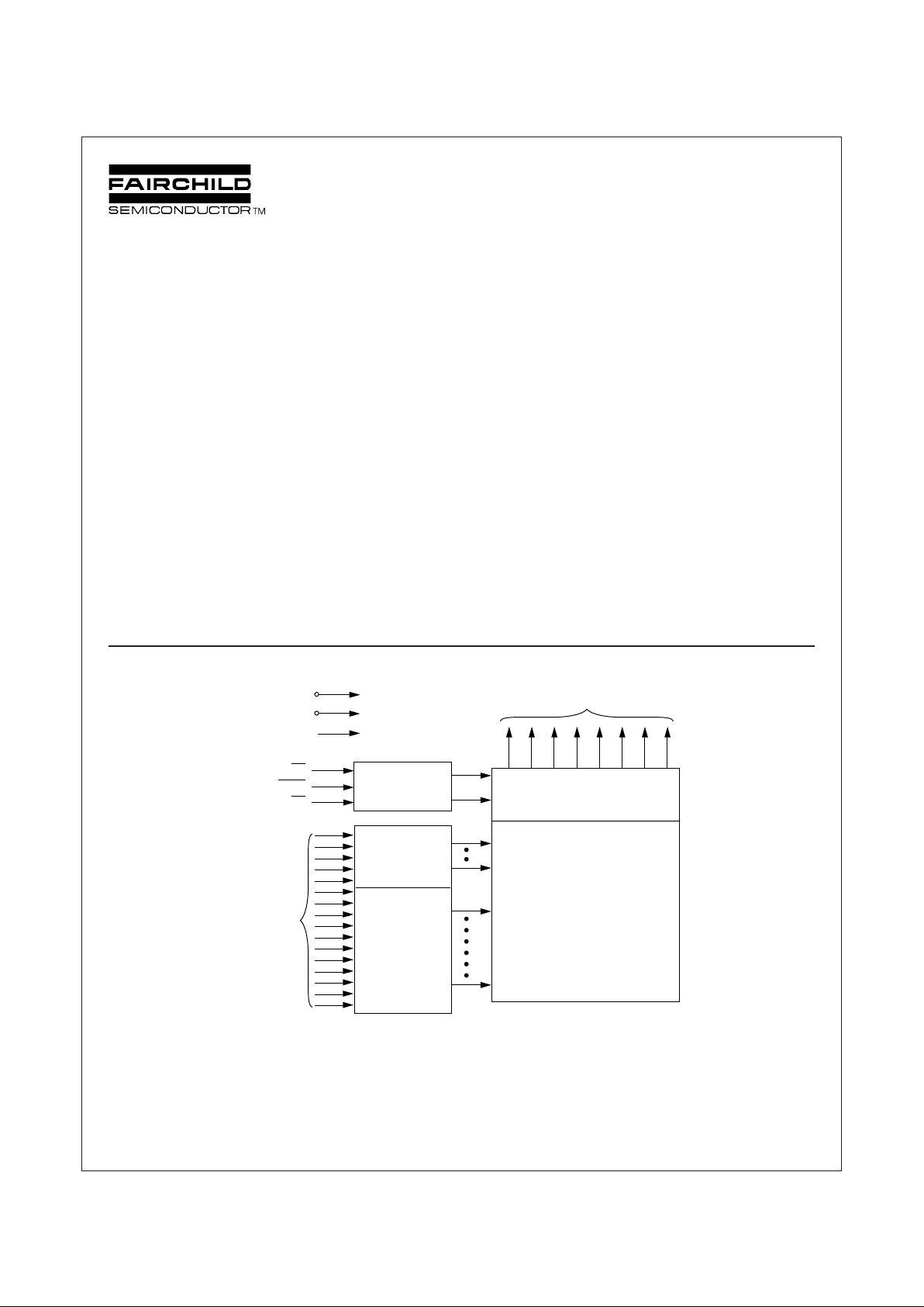
Block Diagram
July 1998
Features
■ 3.0V to 3.6V operation
■ 200 ns access time
■ Low current operation
—8 mA ICC active current @ 5 MHz (typ.)
—20µA ICC standby current @ 5 MHz (typ.)
■ Ultra low power operation
—66 µW standby power @ 3.3V
—50 mW active power @ 3.3V
■ Surface mount package options|
—32-pin TSOP
—32-pin PLCC
DS011377-1
AMG™ is a trademark of WSI, Incorporated.
© 1998 Fairchild Semiconductor Corporation
V
cc
GND
V
pp
OE
Output Enable,
Chip Enable &
Program Logic
Y
Decoder
X
Decoder
Output
Buffers
1,048,576-Bit
Cell Matrix
A
0 - A16
Address
Inputs
Data Outputs O
0 - O7
CE
PGM
2
www.fairchildsemi.com
NM27LV010 1,048,576-Bit (128k x 8) Low Voltage EPROM
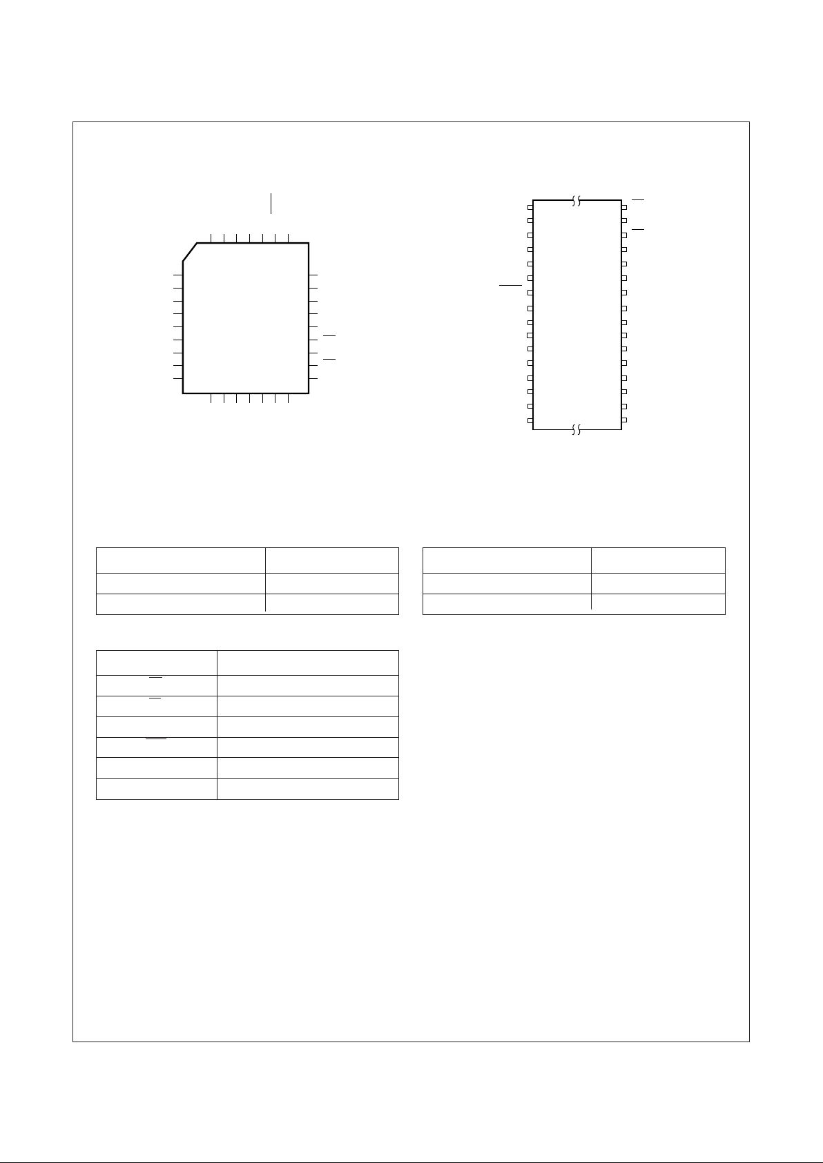
Connection Diagrams
PLCC Pin Configuration
Top View
TSOP Pin Configuration
Top View
Commercial Temperature Range
(0°C to +70°C) VCC = 3.3 ± 0.3
Parameter/Order Number Access Time (ns)
NM27LV010 V, T 200 200
NM27LV010 V, T 250 250
Pin Names
A0–A16 Addresses
CE Chip Enable
OE Output Enable
O0–O7 Outputs
PGM Program
XX Don’t Care (During Read)
V
PP
Programming Voltage
Industrial Temperature Range
(-40°C to +85°C) VCC = 3.3 ± 0.3
Parameter/Order Number Access Time (ns)
NM27LV010 VE, TE 200
NM27LV010 VE, TE 250
Package Types: NM27LV010 V, T
V = PLCC
T = TSOP
• All packages conform to the JEDEC standard.
• All versions are guaranteed to function for slower speeds.
• Consult the Fairchild Sales office on new released products
and packages.
• Consult the Fairchild representative for custom products for
your specific application.
A
14
A
13
A
8
A
9
A
11
OE
A
10
CE
O
7
A
7
A
6
A
5
A
4
A
3
A
2
A
1
A
0
O
0
A12A15A16XX/VPPVCCXX/PGM
XX
O1O
2
GND
O3O4O5O
6
5
6
7
8
9
10
11
12
13
29
28
27
26
25
24
23
22
21
14 15 16 17 18 19 20
4 3 2 1 32 31 30
A
11
A
9
A
8
A
13
A
14
NC
PGM
V
CC
V
PP
A
16
A
15
A
12
A
7
A
6
A
5
A
4
OE
A
10
CE
O7
O
6
O
5
O4
O
3
V
SS
O
2
O1
O
0
A
0
A
1
A
2
A
3
1
2
3
4
5
6
7
8
9
10
11
12
13
14
15
16
32
31
30
29
28
27
26
25
24
23
22
21
20
19
18
17
8 x 20 MM
TSOP
DS011377-2
DS011377-6
3
www.fairchildsemi.com
NM27LV010 1,048,576-Bit (128k x 8) Low Voltage EPROM
Absolute Maximum Ratings (Note 1)
Storage Temperature -65°C to +150°C
All Input Voltages except A9 with
Respect to Ground (Note 10) -0.6V to +7V
VPP and A9 with Respect to Ground -0.6V to +14V
VCC Supply Voltage with
Respect to Ground -0.6V to +7V
ESD Protection >2000V
All Output Voltages with VCC + 1.0V
Respect to Ground (Note 10) to GND - 0.6V
Operating Range
Range Temperature V
CC
Tolerance
Commercial 0°C to +70°C 3.3V ±0.3V
Industrial -40°C to +85°C 3.3V ±0.3V
DC Electrical Characteristics Over Operating Range with V
PP
= V
CC
Symbol Parameter Test Conditions Min Max Units
V
IL
Input Low Level -0.3 0.7 V
V
IH
Input High Level 2.0 VCC + 0.3 V
V
OL1
Output Low Voltage (TTL) IOL = 2.0 mA 0.4 V
V
OH1
Output High Voltage (TTL) IOH = -2.0 mA 2.4 V
V
OL2
Output Low Voltage IOL = 100 µA 0.2 V
V
OH2
Output High Voltage (CMOS) IOH = -100 µAV
CC
- 0.3
I
SB1
VCC Standby Current CE = VCC ± 0.3V 50 µA
(CMOS)
I
SB2
VCC Standby Current (TTL) CE = V
IH
100 µA
I
CC
VCC Active Current CE = OE = VIL, f = 5 MHz 15 mA
I/O = 0 µA
I
PP
VPP Supply Current VPP = V
CC
10 µA
V
PP
VPP Read Voltage VCC - 0.7 V
CC
V
I
LI
Input Load Current VIN = 3.0V or GND 1 µA
I
LO
Output Leakage Current V
OUT
= 3.0V or GND -1 10 µA
AC Electrical Characteristics Over Operating Range with V
PP
= V
CC
Symbol Parameter 200 250 Units
Min Max Min Max
t
ACC
Address to Output Delay 200 250 ns
t
CE
CE to Output Delay 200 250
t
OE
OE to Output Delay 70 75
t
DF
Output Disable to Output Float 50 50
(Note 2)
t
OH
Output Hold from Addresses,
(Note 2) CE or OE , Whichever 0 0
Occurred First
 Loading...