

Fairchild Semiconductor NM24W04EM8X, NM24W04LEM8, NM24W04LEM8X, NM24W04LMT8, NM24W04N Datasheet
...
1
www.fairchildsemi.com
NM24Wxx Rev. C.2
NM24Wxx 2K/4K/8K/16K-Bit Standard 2-Wire Bus Interface
Serial EEPROM with Full Array Write Protect
PRELIMINARY
March 1999
© 1999 Fairchild Semiconductor Corporation
NM24Wxx
2K/4K/8K/16K-Bit Standard 2-Wire Bus Interface
Serial EEPROM with Full Array Write Protect
General Description
The NM24Wxx devices are 2048/4096/8192/16,384 bits, respectively, of CMOS non-volatile electrically erasable memory. These
devices conform to all specifications in the IIC 2-wire protocol and
are designed to minimize device pin count, and simplify PC board
layout requirements.
The entire ememory can be disabled (Write Protected) by connecting the WP pin to VCC. The memory then becomes unalterable
unless WP is switched to VSS.
This communications protocol uses CLOCK (SCL) and DATA
I/O (SDA) lines to synchronously clock data between the master
(for example a microprocessor) and the slave EEPROM device(s).
The Standard IIC protocol allows for a maximum of 16K of
EEPROM memory which is supported by Fairchild's family in 2K,
4K, 8K, and 16K devices, allowing the user to configure the
memory as the application requires with any combination of
EEPROMs.
Fairchild EEPROMs are designed and tested for applications
requiring high endurance, high reliability and low power consumption.
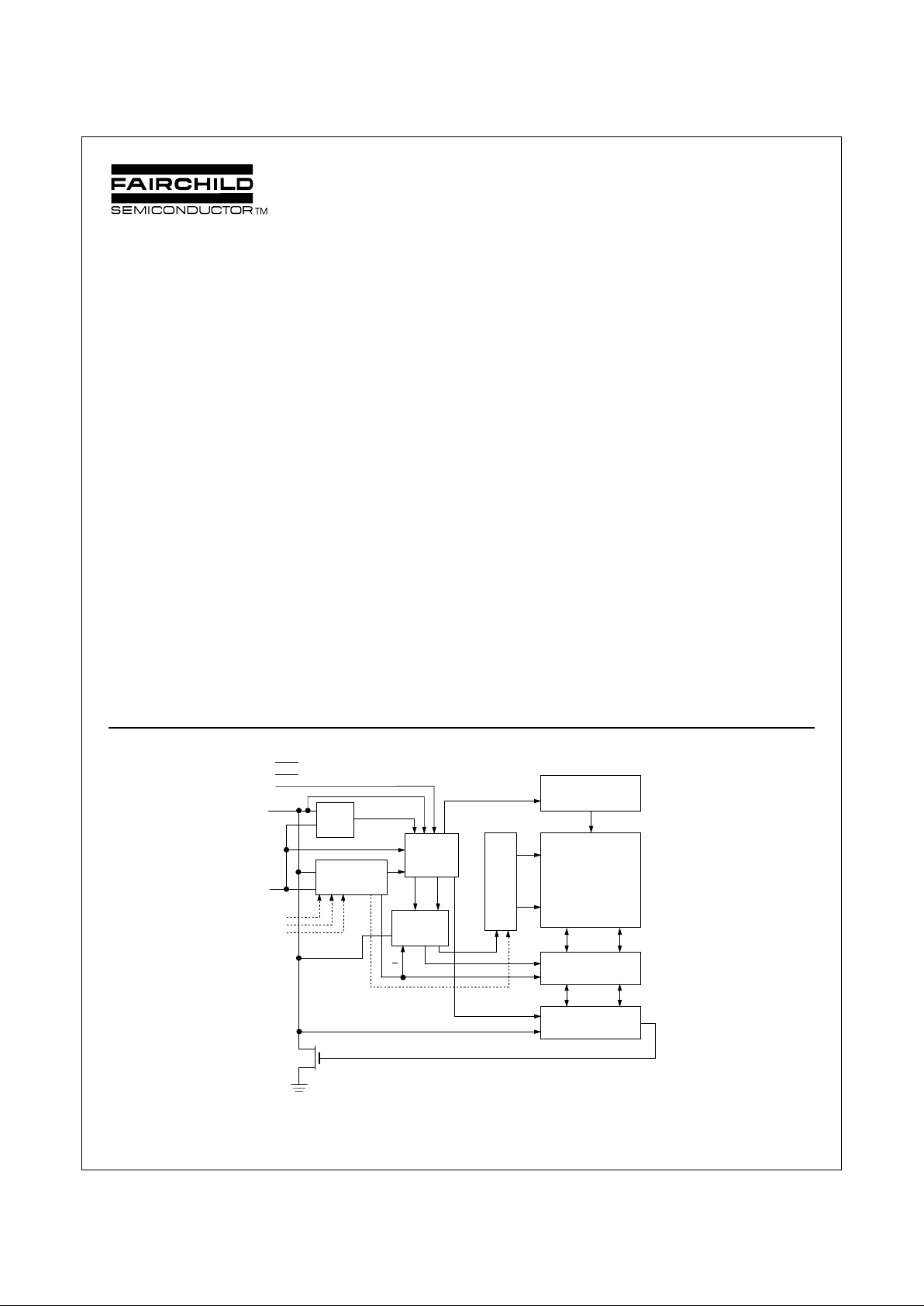
Block Diagram
DS500074-1
H.V. GENERATION
TIMING &CONTROL
E2PROM
ARRAY
16
YDEC
8
DATA REGISTER
XDEC
CONTROL
LOGIC
WORD
ADDRESS
COUNTER
SLAVE ADDRESS
REGISTER &
COMPARATOR
START
STOP
LOGIC
START CYCLE
16/
32/
64/
128/
4
4
CK
D
IN
R/W
LOAD INC
SDA
V
SS
V
CC
WP
D
OUT
A2
A1
A0
Device Address Bits
0/1/2/3
SCL
Features
■ Hardware Write Protect for entire memory
■ Low Power CMOS
200µA active current typical
10µA standby current typical
1µA standby typical (L)
0.1µA standby typical (LZ)
■ IIC Compatible interface
— Provides bidirectional data transfer protocol
■ Sixteen byte page write mode
— Minimizes total write time per byte
■ Self timed write cycle
— Typical write cycle time of 6ms
■ Endurance: 1,000,000 data changes
■ Data retention greater than 40 years
■ Packages available: 8-pin DIP, 8-pin SO, and 8-pin TSSOP
■ Available in three temperature ranges
- Commercial: 0° to +70°C
- Extended (E): -40° to +85C
- Automotive (V): -40° to +125°C
2
www.fairchildsemi.com
NM24Wxx Rev. C.2
NM24Wxx 2K/4K/8K/16K-Bit Standard 2-Wire Bus Interface
Serial EEPROM with Full Array Write Protect
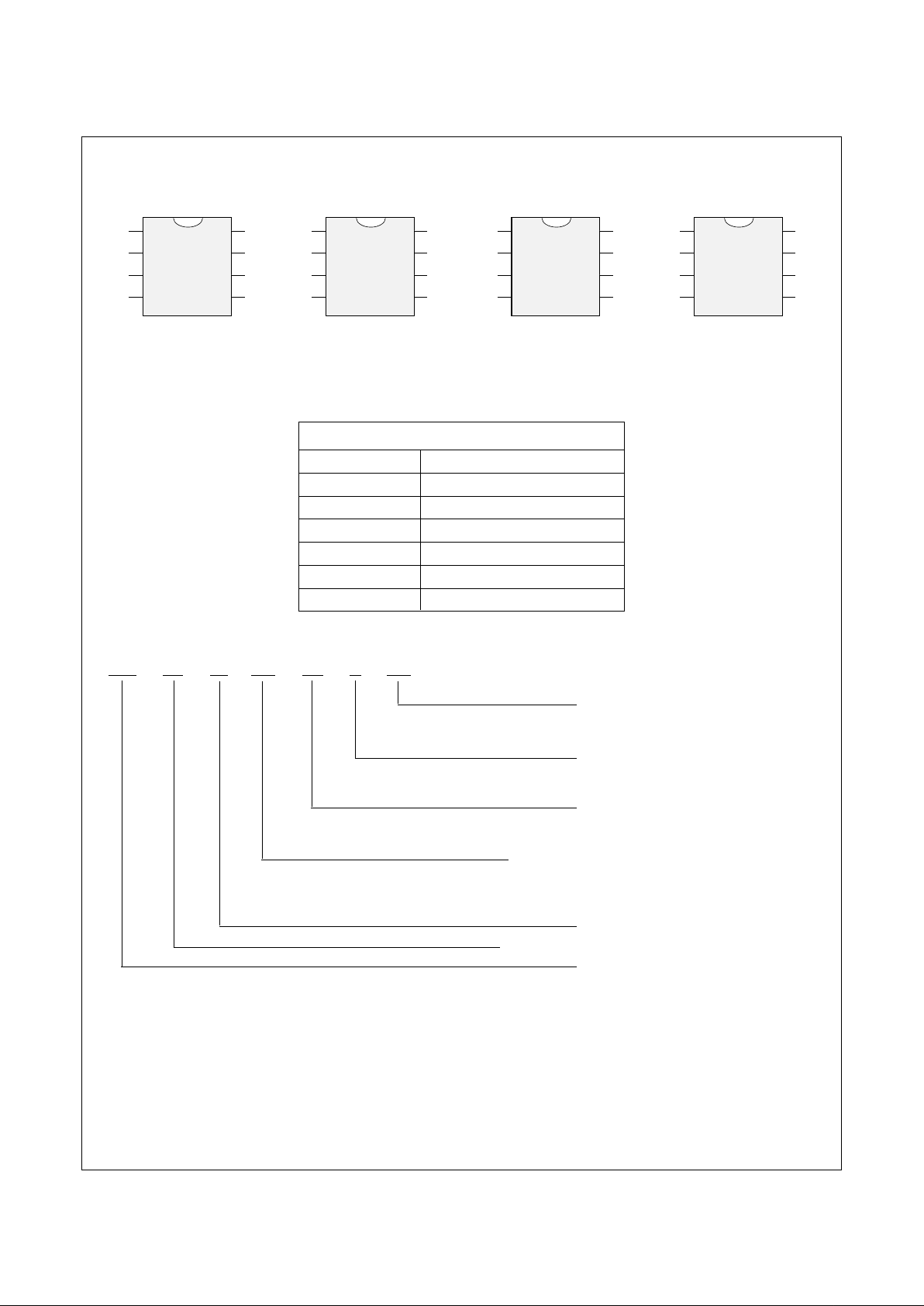
Connection Diagrams
Dual-In-Line Package (N), SO Package (M8), and TSSOP Package (MT8)
Top View
See Package Number N08E (N), M08A (M8), and MTC08 (MT8)
Pin Names
A0,A1,A2 Device Address Inputs
V
SS
Ground
SDA Data I/O
SCL Clock Input
WP Write Protect
V
CC
Power Supply
NC No Connect
Ordering Information
NM 24 W XX LZ E XX Letter Description
Package N 8-Pin DIP
M8 8-Pin SO8
MT8 8-Pin TSSOP
Temp. Range None 0 to 70°C
E -40 to +85°C
V -40°C to +125°C
Voltage Operating Range Blank 4.5V to 5.5V
L 2.7V to 4.5V
LZ 2.7V to 4.5V and
<1µA Standby Current
Density 02 2K
04 4K
08 8K
16 16K
W Total Array Write Protect
Interface 24 IIC
NM Fairchild Non-Volatile
Memory
A0
A1
A2
V
SS
V
CC
WP
SCL
SDA
8
7
6
5
1
2
3
4
DS500074-3
NM24W02
NC
A1
A2
V
SS
V
CC
WP
SCL
SDA
8
7
6
5
1
2
3
4
NC
NC
A2
V
SS
V
CC
WP
SCL
SDA
8
7
6
5
1
2
3
4
NC
NC
NC
V
SS
V
CC
WP
SCL
SDA
8
7
6
5
1
2
3
4
NM24W04 NM24W08 NM24W16
DS500074-4 DS500074-18DS500074-2
3
www.fairchildsemi.com
NM24Wxx Rev. C.2
NM24Wxx 2K/4K/8K/16K-Bit Standard 2-Wire Bus Interface
Serial EEPROM with Full Array Write Protect
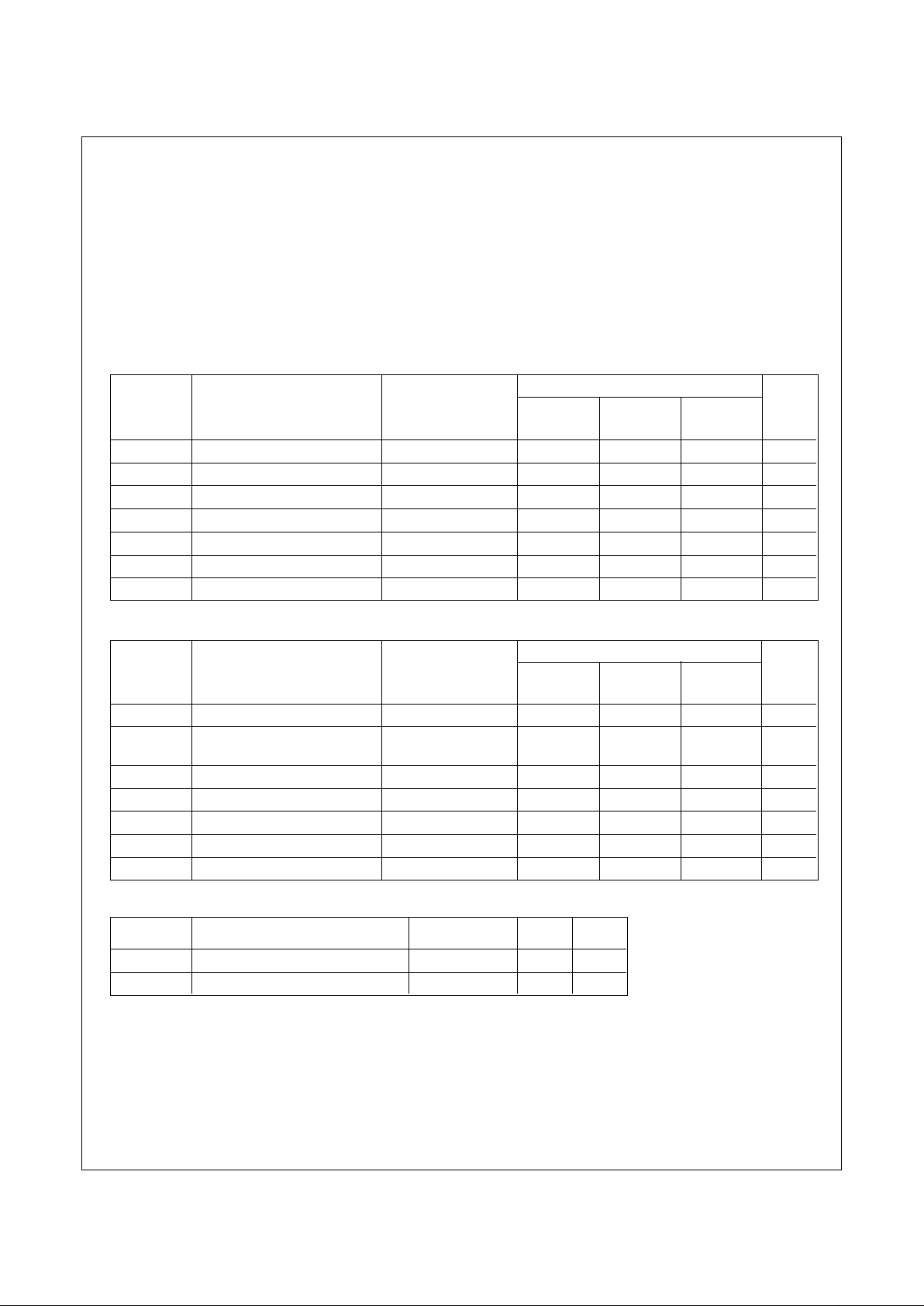
Product Specifications
Absolute Maximum Ratings
Ambient Storage Temperature –65°C to +150°C
All Input or Output Voltages
with Respect to Ground 6.5V to –0.3V
Lead Temperature
(Soldering, 10 seconds) +300°C
ESD Rating 2000V min.
Operating Conditions
Ambient Operating Temperature
NM24Wxx 0°C to +70°C
NM24WxxE -40°C to +85°C
NM24WxxV -40°C to +125°C
Positive Power Supply
NM24Wxx 4.5V to 5.5V
NM24WxxL 2.7V to 4.5V
NM24WxxLZ 2.7V to 4.5V
Standard VCC (4.5V to 5.5V) DC Electrical Characteristics
Symbol Parameter Test Conditions Limits Units
Min Typ Max
(Note 1)
I
CCA
Active Power Supply Current f
SCL
= 100 kHz 0.2 1.0 mA
I
SB
Standby Current VIN = GND or V
CC
10 50 µA
I
LI
Input Leakage Current VIN = GND to V
CC
0.1 1 µA
I
LO
Output Leakage Current V
OUT
= GND to V
CC
0.1 1 µA
V
IL
Input Low Voltage –0.3 VCC x 0.3 V
V
IH
Input High Voltage VCC x 0.7 VCC + 0.5 V
V
OL
Output Low Voltage I
OL
= 3 mA 0.4 V
Low VCC (2.7V to 5.5V) DC Electrical Characteristics
Symbol Parameter Test Conditions Limits Units
Min Typ Max
(Note 1)
I
CCA
Active Power Supply Current f
SCL
= 100 kHz 0.2 1.0 mA
I
SB
Standby Current for L VIN = GND or V
CC
110µA
Standby Current for LZ VIN = GND or V
CC
0.1 1 µA
I
LI
Input Leakage Current VIN = GND to V
CC
0.1 1 µA
I
LO
Output Leakage Current V
OUT
= GND to V
CC
0.1 1 µA
V
IL
Input Low Voltage –0.3 V
CC
x 0.3 V
V
IH
Input High Voltage VCC x 0.7 VCC + 0.5 V
V
OL
Output Low Voltage IOL = 3 mA 0.4 V
Capacitance T
A
= +25°C, f = 100/400 KHz, VCC = 5V (Note 2)
Symbol Test Conditions Max Units
C
I/O
Input/Output Capacitance (SDA) V
I/O
= 0V 8 pF
C
IN
Input Capacitance (A0, A1, A2, SCL) VIN = 0V 6 pF
Note 1: Typical values are TA = 25°C and nominal supply voltage (5V).
Note 2: This parameter is periodically sampled and not 100% tested.
4
www.fairchildsemi.com
NM24Wxx Rev. C.2
NM24Wxx 2K/4K/8K/16K-Bit Standard 2-Wire Bus Interface
Serial EEPROM with Full Array Write Protect
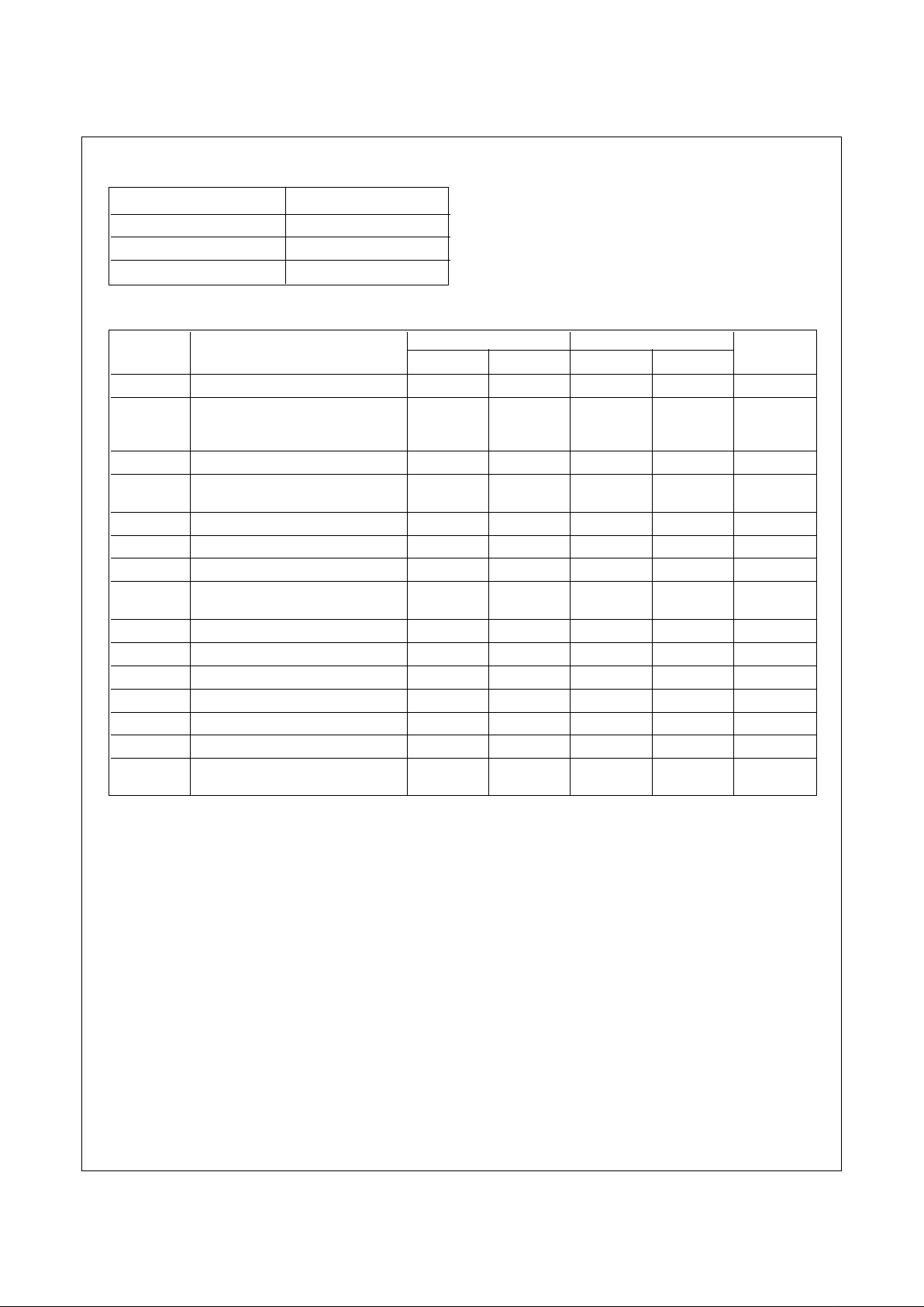
AC Conditions of Test
Input Pulse Levels VCC x 0.1 to VCC x 0.9
Input Rise and Fall Times 10 ns
Input & Output Timing Levels VCC x 0.5
Output Load 1 TTL Gate and CL = 100 pF
Read and Write Cycle Limits (Standard and Low VCC Range 2.7V - 4.5V)
Symbol Parameter 100 KHz 400 KHz Units
Min Max Min Max
f
SCL
SCL Clock Frequency 100 400 KHz
T
I
Noise Suppression Time Constant at
SCL, SDA Inputs (Minimum V
IN
100 50 ns
Pulse width)
t
AA
SCL Low to SDA Data Out Valid 0.3 3.5 0.1 0.9 µs
t
BUF
Time the Bus Must Be Free before 4.7 1.3 µs
a New Transmission Can Start
t
HD:STA
Start Condition Hold Time 4.0 0.6 µs
t
LOW
Clock Low Period 4.7 1.5 µs
t
HIGH
Clock High Period 4.0 0.6 µs
t
SU:STA
Start Condition Setup Time 4.7 0.6 µs
(for a Repeated Start Condition)
t
HD:DAT
Data in Hold Time 0 0 ns
t
SU:DAT
Data in Setup Time 250 100 ns
t
R
SDA and SCL Rise Time 1 0.3 µs
t
F
SDA and SCL Fall Time 300 300 ns
t
SU:STO
Stop Condition Setup Time 4.7 0.6 µs
t
DH
Data Out Hold Time 300 50 ns
t
WR
Write Cycle Time - NM24Wxx 10 10 ms
(Note 3) - NM24WxxL, NM24WxxLZ 15 15
Note 3: The write cycle time (tWR) is the time from a valid stop condition of a write sequence to the end of the internal erase/program cycle. During the write cycle, the
NM24Wxx bus interface circuits are disabled, SDA is allowed to remain high per the bus-level pull-up resistor, and the device does not respond to its slave address.
5
www.fairchildsemi.com
NM24Wxx Rev. C.2
NM24Wxx 2K/4K/8K/16K-Bit Standard 2-Wire Bus Interface
Serial EEPROM with Full Array Write Protect
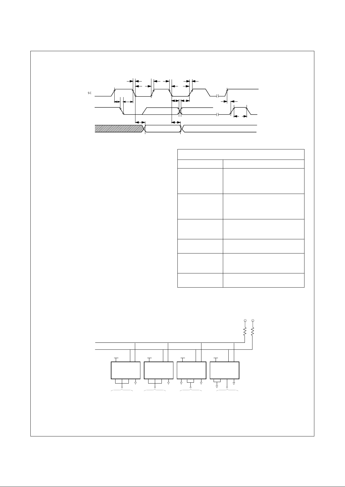
Bus Timing
Background Information (IIC Bus)
As mentioned, the IIC bus allows synchronous bidirectional communication between Transmitter/Receiver using the SCL (clock)
and SDA (Data I/O) lines. All communication must be started with
a valid START condition, concluded with a STOP condition and
acknowledged by the Receiver with an ACKNOWLEDGE condition.
In addition, since the IIC bus is designed to support other devices
such as RAM, EPROMs, etc., a devce type identifier string must
follow the START condition. For EEPROMs, this 4-bit string is
1010 and is the first 4 bits in the slave address.
As shown below, the EEPROMs on the IIC bus may be configured
in any manner required, and for the Standard IIC protocol, the total
memory addressed can not exceed 16K (16,384 bits). EEPROM
memory address programming is controlled by 2 methods:
• Hardware configuring the A0, A1, and A2 pins (Device
Address pins) with pull-up or pull-down to resistors. All
unused pins must be grounded (tied to VSS).
• Software addressing the required PAGE BLOCK within the
device memory array (as sent in the Slave Address string).
Addressing an EEPROM memory location involves sending a
command string with the following information:
[DEVICE TYPE]—[DEVICE ADDRESS]—[PAGE BLOCK
ADDRESS]—[BYTE ADDRESS]
DEFINITIONS
WORD 8 bits of data
PAGE 16 sequential addresses (one byte
each) that may be programmed
during a 'Page Write' programming
cycle
PAGE BLOCK 2,048 (2K) bits organized into 16
pages of addressable memory. (8
bits) x (16 bytes) x (16 pages) = 2,048
bits
MASTER Any IIC device CONTROLLING the
transfer of data (such as a microprocessor)
SLAVE Device being controlled (EEPROMs
are always considered Slaves)
TRANSMITTER Device currently SENDING data on
the bus (may be either a Master or
Slave).
RECEIVER Device currently receiving data on the
bus (Master or Slave)
Example of 16K of Memory on 2-Wire Bus
Note: The SDA pull-up resistor is required due to the open-drain/open collector output of IIC bus devices.
The SCL pull-up resistor is recommended because of the normal SCL line inactive 'high' state.
It is recommended that the total line capacitance be less than 400pF.
Specific timing and addressing considerations are described in greater detail in the following sections.
DS500074-5
DS500074-6
SDA
SCL
NM24W02
V
CC
V
CC
A0 A1 A2 V
SS
NM24W02
A0 A1 A2 V
SS
NM24W04
A0 A1 A2 V
SS
NM24W08
A0 A1 A2 V
SS
V
CC
To V
CC
or V
SS
To V
CC
or V
SS
To V
CC
or V
SS
To V
CC
or V
SS
V
CC
V
CC
V
CC
SCL
SDA
IN
SDA
OUT
t
F
t
LOW
t
HIGH
t
R
t
LOW
t
AA
t
DH
t
BUF
t
SU:STA
t
HD:DAT
t
HD:STA
t
SU:DAT
t
SU:STO
 Loading...