

Fairchild Semiconductor NM24C65UDWF, NM24C65UEM8, NM24C65ULZN, NM24C65UM8, NM24C65UVM8X Datasheet
...
1
www.fairchildsemi.com
NM24C65U Rev. B.1
NM24C65U 64K-Bit Serial EEPROM with Write Protect 2-Wire Bus Interface
PRELIMINARY
August 1999
© 1999 Fairchild Semiconductor Corporation
NM24C65U
64K-Bit Serial EEPROM with Write Protect
2-Wire Bus Interface
General Description:
The NM24C65U is a 64K (65,536) bit serial interface CMOS
EEPROM (Electrically Erasable Programmable Read-Only
Memory). This device fully conforms to the Extended I2C™ 2-wire
protocol which uses Clock (SCL) and Data I/O (SDA) pins to
synchronously clock data between the "master" (for example a
microprocessor) and the "slave" (the EEPROM device). In addition, the serial interface allows a minimal pin count packaging
designed to simplify PC board layout requirements and offers the
designer a variety of low voltage and low power options.
NM24C65U incorporates a hardware "Write Protect" feature, by
which the upper half of the memory can be disabled against
programming by connecting the WP pin to VCC. This section of
memory then effectively becomes a ROM (Read-Only Memory)
and can no longer be programmed as long as WP pin is connected
to VCC.
Fairchild EEPROMs are designed and tested for applications requiring high endurance, high reliability and low power consumption for a
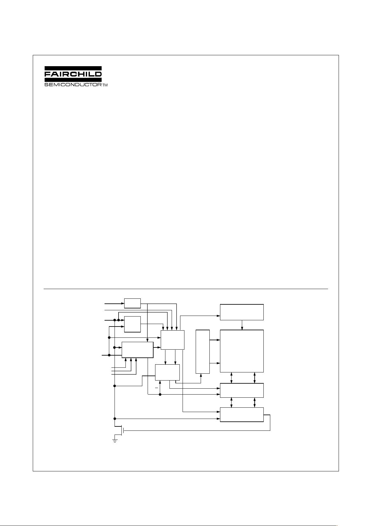
Block Diagram
continuously reliable non-volatile solution for all markets.
Functions
■ I2C™ compatible interface
■ 65,536 bits organized as 8,192 x 8
■ 100 KHz or 400 KHz operation
■ Extended 2.7V – 5.5V operating voltage
■ Self timed programming cycle (6ms typical)
■ "Programming complete" indicated by ACK polling
■ Memory "Upper Block" Write Protect pin
Features
■ The I2C™ interface allows the smallest I/O pincount of any
EEPROM interface
■ 32 byte page write mode to minimize total write time per byte
■ Low VCC programming lockout (3.8V)
— "H" option (Standard VCC range) parts only
■ Typical 200µA active current (I
CCA
)
■ Typical 1µA standby current (ISB) for "L" devices and 0.1µA
standby current for "LZ" devices
■ Endurance: Up to 1,000,000 data changes
■ Data retention greater than 40 years
DS800012-1
H.V. GENERATION
TIMING &CONTROL
E2PROM
ARRAY
YDEC
DATA REGISTER
XDEC
CONTROL
LOGIC
WORD
ADDRESS
COUNTER
SLAVE ADDRESS
REGISTER &
COMPARATOR
START
STOP
LOGIC
WRITE
LOCKOUT
START CYCLE
CK
D
IN
R/W
LOAD INC
SDA
SCL
WP
V
CC
D
OUT
A2
A1
A0
I2C™ is a registered trademark of Philips Electronics N.V.
2
www.fairchildsemi.com
NM24C65U Rev. B.1
NM24C65U 64K-Bit Serial EEPROM with Write Protect 2-Wire Bus Interface
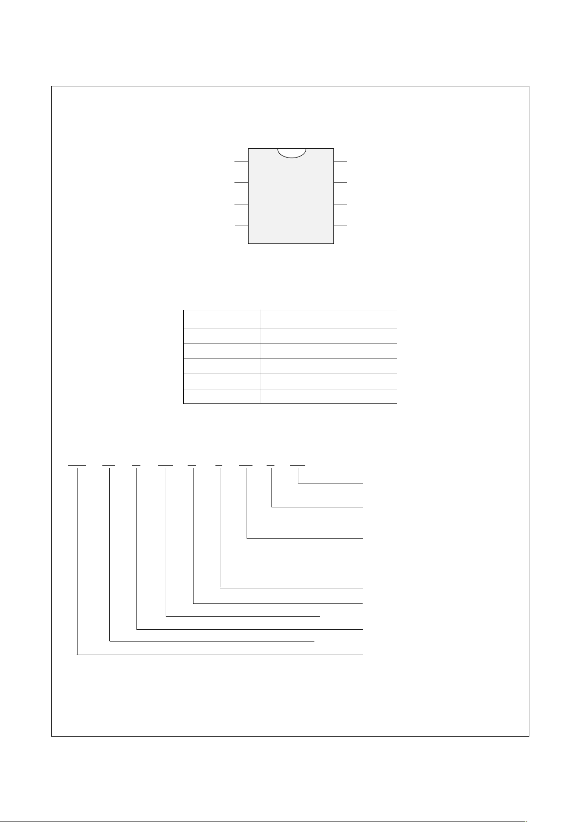
Connection Diagram
Dual-In-Line Package (N)
and 8-Pin SO Package (M8)
Top View
See Package Number N08E and M08A
Pin Names
A0, A1, A2 Device Address Input
V
SS
Ground
SDA Data I/O
SCL Clock Input
WP Write Protect
V
CC
Power Supply
Ordering Information
NM 24 C XX U F LZ E XX Letter Description
Package N 8-Pin DIP
M8 8-Pin SOIC
Temp. Range None 0 to 70°C
V -40 to +125°C
E -40 to +85°C
Voltage Operating Range Blank 4.5V to 5.5V
L 2.7V to 5.5V
LZ 2.7V to 5.5V and
<1µA Standby Current
H 4.5V to 5.5V and VCC Lockout
SCL Clock Frequency Blank 100KHz
F 400KHz
Ultralite CS100UL Process
Density 65 64K with Write Protect
C CMOS
Interface 24 IIC
NM Fairchild Non-Volatile
Memory
A0
A1
A2
V
SS
V
CC
WP
SCL
SDA
8
7
6
5
1
2
3
4
NM24C65U
DS800012-2
3
www.fairchildsemi.com
NM24C65U Rev. B.1
NM24C65U 64K-Bit Serial EEPROM with Write Protect 2-Wire Bus Interface
Product Specifications
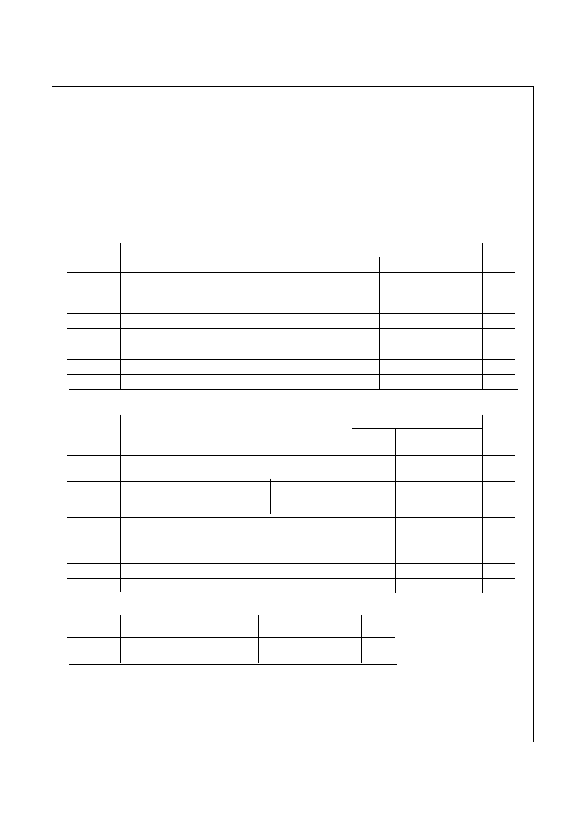
Absolute Maximum Ratings
Ambient Storage Temperature –65°C to +150°C
All Input or Output Voltages
with Respect to Ground 6.5V to –0.3V
Lead Temperature
(Soldering, 10 seconds) +300°C
ESD Rating 2000V min.
Operating Conditions
Ambient Operating Temperature
NM24C65U 0°C to +70°C
NM24C65UE -40°C to +85°C
NM24C65UV -40°C to +125°C
Positive Power Supply
NM24C65U/NM24C65UH 4.5V to 5.5V
NM24C65UL 2.7V to 5.5V
NM24C65ULZ 2.7V to 5.5V
Standard VCC (4.5V to 5.5V) DC Electrical Characteristics
Symbol Parameter Test Conditions Limits Units
Min
Typ (Note 1)
Max
I
CCA
Active Power Supply Current f
SCL
= 400 kHz 0.2 1.0 mA
f
SCL
= 100 kHz
I
SB
Standby Current VIN = GND or V
CC
10 50 µA
I
LI
Input Leakage Current VIN = GND to V
CC
0.1 1 µA
I
LO
Output Leakage Current V
OUT
= GND to V
CC
0.1 1 µA
V
IL
Input Low Voltage –0.3 VCC x 0.3 V
V
IH
Input High Voltage VCC x 0.7 VCC + 0.5 V
V
OL
Output Low Voltage I
OL
= 3 mA 0.4 V
Low VCC (2.7V to 5.5V) DC Electrical Characteristics
Symbol Parameter Test Conditions Limits Units
Min Typ Max
(Note 1)
I
CCA
Active Power Supply Current f
SCL
= 400 KHz 0.2 1.0 mA
f
SCL
= 100 KHz
I
SB
Standby Current VIN = GND VCC = 2.7V - 4.5V 1 10 µA
or V
CC
VCC = 2.7V - 4.5V 0.1 1 µA
VCC = 4.5V - 5.5V 10 50 µA
I
LI
Input Leakage Current VIN = GND to V
CC
0.1 1 µA
I
LO
Output Leakage Current V
OUT
= GND to V
CC
0.1 1 µA
V
IL
Input Low Voltage –0.3 V
CC
x 0.3 V
V
IH
Input High Voltage VCC x 0.7 VCC + 0.5 V
V
OL
Output Low Voltage IOL = 3 mA 0.4 V
Capacitance T
A
= +25°C, f = 100/400 KHz, VCC = 5V (Note 2)
Symbol Test Conditions Max Units
C
I/O
Input/Output Capacitance (SDA) V
I/O
= 0V 8 pF
C
IN
Input Capacitance (A0, A1, A2, SCL) VIN = 0V 6 pF
Note 1: Typical values are for TA = 25°C and nominal supply voltage (5V).
Note 2: This parameter is periodically sampled and not 100% tested.

4
www.fairchildsemi.com
NM24C65U Rev. B.1
NM24C65U 64K-Bit Serial EEPROM with Write Protect 2-Wire Bus Interface
AC Conditions of Test
Input Pulse Levels VCC x 0.1 to VCC x 0.9
Input Rise and Fall Times 10 ns
Input & Output Timing Levels VCC x 0.5
Output Load 1 TTL Gate and CL = 100 pF
Read and Write Cycle Limits (Standard and Low VCC Range - 2.7V-5.5V)
Symbol Parameter 100 KHz 400 KHz Units
Min Max Min Max
f
SCL
SCL Clock Frequency 100 400 KHz
T
I
Noise Suppression Time Constant at
SCL, SDA Inputs (Minimum V
IN
100 50 ns
Pulse width)
t
AA
SCL Low to SDA Data Out Valid 0.3 3.5 0.1 0.9 µs
t
BUF
Time the Bus Must Be Free before 4.7 1.3 µs
a New Transmission Can Start
t
HD:STA
Start Condition Hold Time 4.0 0.6 µs
t
LOW
Clock Low Period 4.7 1.5 µs
t
HIGH
Clock High Period 4.0 0.6 µs
t
SU:STA
Start Condition Setup Time 4.7 0.6 µs
(for a Repeated Start Condition)
t
HD:DAT
Data in Hold Time 0 0 µs
t
SU:DAT
Data in Setup Time 250 100 ns
t
R
SDA and SCL Rise Time 1 0.3 µs
t
F
SDA and SCL Fall Time 300 300 ns
t
SU:STO
Stop Condition Setup Time 4.7 0.6 µs
t
DH
Data Out Hold Time 300 50 ns
t
WR
Write Cycle Time - NM24C65U 10 10 ms
(Note 3) - NM24C65UL, NM24C65ULZ 15 15
Note 3: The write cycle time (tWR) is the time from a valid stop condition of a write sequence to the end of the internal erase/program cycle. During the write cycle, the
NM24C65U bus interface circuits are disabled, SDA is allowed to remain high per the bus-level pull-up resistor, and the device does not respond to its slave address
 Loading...