


Fairchild Semiconductor NM24C16UVM8, NM24C16UTLMT8X, NM24C16UEN, NM24C16ULMT8, NM24C16ULM8X Datasheet
...
1
www.fairchildsemi.com
NM24C16U/17U Rev. B.1
NM24C16U/NM24C17U – 16K-Bit Serial EEPROM 2-Wire Bus Interface
August 1999
© 1999 Fairchild Semiconductor Corporation
NM24C16U/NM24C17U
16K-Bit Serial EEPROM
2-Wire Bus Interface
General Description
The NM24C16U/17U devices are 16K (16,384) bit serial interface
CMOS EEPROMs (Electrically Erasable Programmable ReadOnly Memory). These devices fully conform to the Standard I2C™
2-wire protocol which uses Clock (SCL) and Data I/O (SDA) pins
to synchronously clock data between the "master" (for example a
microprocessor) and the "slave" (the EEPROM device). In addition, the serial interface allows a minimal pin count packaging
designed to simplify PC board layout requirements and offers the
designer a variety of low voltage and low power options.
NM24C17U incorporates a hardware "Write Protect" feature, by
which, the upper half of the memory can be disabled against
programming by connecting the WP pin to VCC. This section of
memory then effectively becomes a ROM (Read-Only Memory)
and can no longer be programmed as long as WP pin is connected
to VCC.
Fairchild EEPROMs are designed and tested for applications requiring high endurance, high reliability and low power consumption for a
continuously reliable non-volatile solution for all markets.
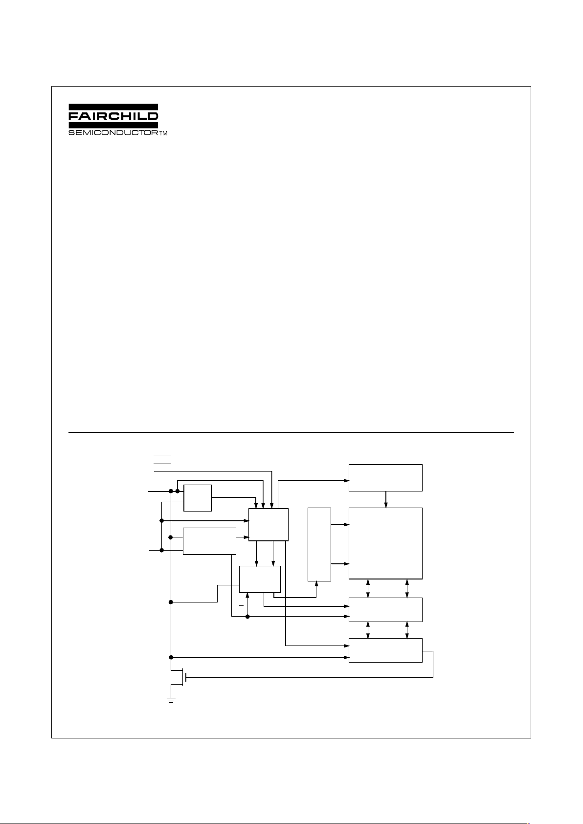
Block Diagram
Functions
■ I2C™ compatible interface
■ 4,096 bits organized as 512 x 8
■ Extended 2.7V – 5.5V operating voltage
■ 100 KHz or 400 KHz operation
■ Self timed programming cycle (6ms typical)
■ "Programming complete" indicated by ACK polling
■ NM24C17U: Memory "Upper Block" Write Protect pin
Features
■ The I2C™ interface allows the smallest I/O pincount of any
EEPROM interface
■ 16 byte page write mode to minimize total write time per byte
■ Typical 200µA active current (I
CCA
)
■ Typical 1µA standby current (ISB) for "L" devices and 0.1µA
standby current for "LZ" devices
■ Endurance: Up to 1,000,000 data changes
■ Data retention greater than 40 years
H.V. GENERATION
TIMING &CONTROL
E2PROM
ARRAY
YDEC
DATA REGISTER
XDEC
CONTROL
LOGIC
WORD
ADDRESS
COUNTER
SLAVE ADDRESS
REGISTER &
COMPARATOR
START
STOP
LOGIC
CK
D
IN
R/W
SDA
SCL
V
SS
WP
V
CC
D
OUT
DS800010-1
I2C™ is a registered trademark of Philips Electronics N.V.
2
www.fairchildsemi.com
NM24C16U/17U Rev. B.1
NM24C16U/NM24C17U – 16K-Bit Serial EEPROM 2-Wire Bus Interface
Connection Diagrams
Dual-In-Line Package (N),
8-Pin SO Package (M8)
Top View
See Package Number N08E,
M08A and MTC08
Pin Names
V
SS
Ground
SDA Serial Data I/O
SCL Serial Clock Input
NC No Connection
V
CC
Power Supply
Dual-In-Line Package (N),
8-Pin SO Package (M8)
Top View
See Package Number N08E,
M08A and MTC08
Pin Names
V
SS
Ground
SDA Serial Data I/O
SCL Serial Clock input
WP Write Protect
V
CC
Power Supply
NC No Connection
NC
NC
NC
V
SS
V
CC
WP
SCL
SDA
8
7
6
5
1
2
3
4
NC
NC
NC
V
SS
V
CC
NC
SCL
SDA
8
7
6
5
1
2
3
4
NM24C16U
NM24C17U
DS800010-2
DS800010-4
8-Pin TSSOP Package (MT8)
Rotated Die (24C16UT)
NC
V
CC
NC
NC
SCL
SDA
V
SS
NC
8
7
6
5
1
2
3
4
DS800010-3
NM24C16UT
8-Pin TSSOP Package (MT8)
Rotated Die (24C17UT)
DS800010-5
WP
V
CC
NC
NC
SCL
SDA
V
SS
NC
8
7
6
5
1
2
3
4
NM24C17UT
3
www.fairchildsemi.com
NM24C16U/17U Rev. B.1
NM24C16U/NM24C17U – 16K-Bit Serial EEPROM 2-Wire Bus Interface
Ordering Information
NM 24 C XX U F T LZ E XX Letter Description
Package N 8-pin DIP
M8 8-pin SOIC
MT8 8-pin TSSOP
Temp. Range None 0 to 70°C
V -40 to +125°C
E -40 to +85°C
Voltage Operating Range Blank 4.5V to 5.5V
L 2.7V to 5.5V
LZ 2.7V to 5.5V and
<1µA Standby Current
Blank Normal Pin Out
T Rotated Die Pin Out
SCL Clock Frequency Blank 100KHz
F 400KHz
Ultralite CS100UL Process
Density 16 16K
17 16K with Write Protect
C CMOS Technology
W Total Array Write Protect
Interface 24 IIC
NM Fairchild Non-Volatile
Memory
4
www.fairchildsemi.com
NM24C16U/17U Rev. B.1
NM24C16U/NM24C17U – 16K-Bit Serial EEPROM 2-Wire Bus Interface
Product Specifications
Absolute Maximum Ratings
Ambient Storage Temperature –65°C to +150°C
All Input or Output Voltages
with Respect to Ground 6.5V to –0.3V
Lead Temperature
(Soldering, 10 seconds) +300°C
ESD Rating 2000V min.
Operating Conditions
Ambient Operating Temperature
NM24C16U/17U 0°C to +70°C
NM24C16UE/17UE -40°C to +85°C
NM24C16UV/17UV -40°C to +125°C
Positive Power Supply
NM24C16U/17U 4.5V to 5.5V
NM24C16UL/17UL 2.7V to 5.5V
NM24C16ULZ/17ULZ 2.7V to 5.5V
Standard VCC (4.5V to 5.5V) DC Electrical Characteristics
Symbol Parameter Test Conditions Limits Units
Min Typ Max
(Note 1)
I
CCA
Active Power Supply Current f
SCL
= 400 KHz 0.2 1.0 mA
f
SCL
= 100 KHz
I
SB
Standby Current VIN = GND or V
CC
10 50 µA
I
LI
Input Leakage Current VIN = GND to V
CC
0.1 1 µA
I
LO
Output Leakage Current V
OUT
= GND to V
CC
0.1 1 µA
V
IL
Input Low Voltage –0.3 VCC x 0.3 V
V
IH
Input High Voltage VCC x 0.7 VCC + 0.5 V
V
OL
Output Low Voltage I
OL
= 3 mA 0.4 V
Low VCC (2.7V to 5.5V) DC Electrical Characteristics
Symbol Parameter Test Conditions Limits Units
Min Typ Max
(Note 1)
I
CCA
Active Power Supply Current f
SCL
= 400 KHz 0.2 1.0 mA
f
SCL
= 100 KHz
I
SB
Standby Current VIN = GND VCC = 2.7V - 4.5V 1 10 µA
or V
CC
VCC = 2.7V - 4.5V 0.1 1 µA
VCC = 4.5V - 5.5V 10 50 µA
I
LI
Input Leakage Current VIN = GND to V
CC
0.1 1 µA
I
LO
Output Leakage Current V
OUT
= GND to V
CC
0.1 1 µA
V
IL
Input Low Voltage –0.3 V
CC
x 0.3 V
V
IH
Input High Voltage VCC x 0.7 VCC + 0.5 V
V
OL
Output Low Voltage IOL = 3 mA 0.4 V
Capacitance T
A
= +25°C, f = 100/400 KHz, VCC = 5V (Note 2)
Symbol Test Conditions Max Units
C
I/O
Input/Output Capacitance (SDA) V
I/O
= 0V 8 pF
C
IN
Input Capacitance (A0, A1, A2, SCL) VIN = 0V 6 pF
Note 1: Typical values are TA = 25°C and nominal supply voltage (5V).
Note 2: This parameter is periodically sampled and not 100% tested.