

Fairchild Semiconductor NE558 Datasheet
NE558
Quad Timer
www.fairchildsemi.com
Features
• Wide Supply Voltage Range: 4.5V To 16V
• 100 mA Output Current Per Section
• Edge Triggered Witho ut Coupling Capacitor
• Time Per iod Equals RC
• Output independent Of Trigger Cond i t ion s
Applications
• Quad One-Shot
• Sequential Timing
• Precision Timing
• Time Delay Generation
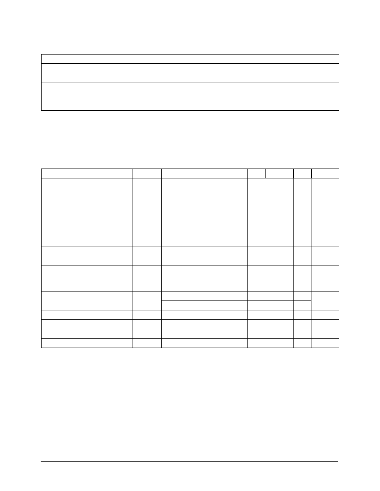
Internal Block Diagram
Description
The NE558 series are monolithic Quad Timers which can
be used to pr oduce four entire ly independent ti ming functions. These highly stable, general purpose controllers can be
used in a monostable mode to produce accurate time de lays,
from microseconds to hours. The time is precisely controlled by one external resistor and one capacitor in the time
delay mode. A stable mode can be operated using two of
four time sections.
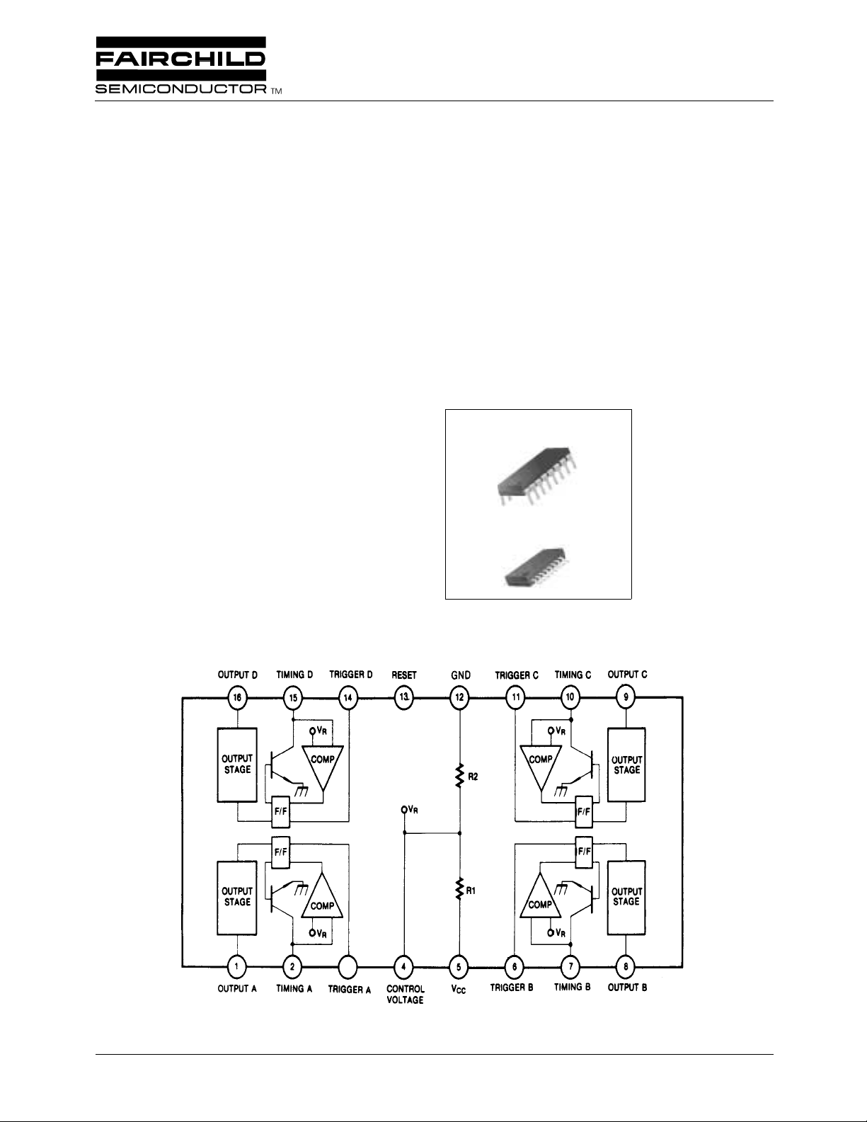
16-DIP
1
16-SOP
1
©2001 Fairchild Semiconductor Corporation
Rev. 1.0.1
NE558
Absolute Maximum Ratings (TA = 25°°°°C)
Parameter Symbol Value Unit
Supply Voltage V
Lead Temperature (soldering 10sec) T
LEAD
Power Dissipation P
Operating Temperature Range NE558 T
Storage Temperature Range T
CC
D
OPR
STG
16 V
300 °C
600 mW
0 ~ + 70 °C
-65 ~ + 150 °C
Electrical Characteristics
(V
= 5 ~ 15V, TA = 25°C, unless otherwise specified)
CC
Parameter Symbol Conditions Min. Typ. Max. Unit
Supply Voltage V
Supply Current I
Timing Error (T = RC)
Initial Accuracy
Drift with Temperature
Drift with Supply Voltage
1
*
Trigger Voltage V
1
*
Trigger Current I
2
Reset Voltage V
*
2
Reset Current I
*
ACCUR
∆t/∆T
∆t/∆V
Threshold Voltage V
Threshold Current I
*3
Output Voltage V
Output Leakage Current I
Propagation Delay Time t
Rise Time t
Fall Time t
CC
CC
TR
TR
RST
RST
TH
TH
O
LKG
D
R
F
VCC =15V, reset voltage =15V - 16 36 mA
R = 2KΩ to 100KΩ, C =1µF-
CC
V
= 15V - 1.5 2.4 V
CC
VTR= 0V - 5.0 100 µA
IL = 10mA - 0.1 0.4
= 100mA - 1.0 2.0
I
L
IL = 100mA - 100 - nS
IL = 100mA - 100 - nS
-4.5-16V
±2
30
0.1
5
150
0.9
- 0.8 1.5 2 .4 V
- - 50 500 µA
-0.8
0.63 ×
V
CC
-V
--15-nA
- - 10 500 nA
--1.0-µS
%
PPM/°C
%/V
V
Note :
1. The trigg er f unctions only on the falling edge of the trigg er pul se o nly after previously being high. After rese t the trigger must
be brought high and then low to implement triggering.
2. For reset below 0.8V, outputs set low and trigger inhibited.
3. Output structure is open collector which requires a pull up resistor to V
The output is normally low sinking current.
to sink current.
CC
2
 Loading...