Fairchild Semiconductor NE556, LM556 Datasheet

LM556/NE556
Dual Timer
www.fairchildsemi.com
Features
• Replaces Two LM555/NE556 Timers
• Operates in Both Astable And Monostable Modes
•High Output Current
• TTL Compatible
• Timing From Microsecond To Hours
• Adjustable Duty Cycle
• Temperature Stability Of 0.005% Per °C
Applications
• Precision Timing
• Pulse Shaping
• Pulse Width Modulation
• Frequency Division
• Traffic Light Control
• Sequential Timing
• Pulse Generator
• Time Delay Generator
• Touch Tone Encoder
• Tone Burst Generator
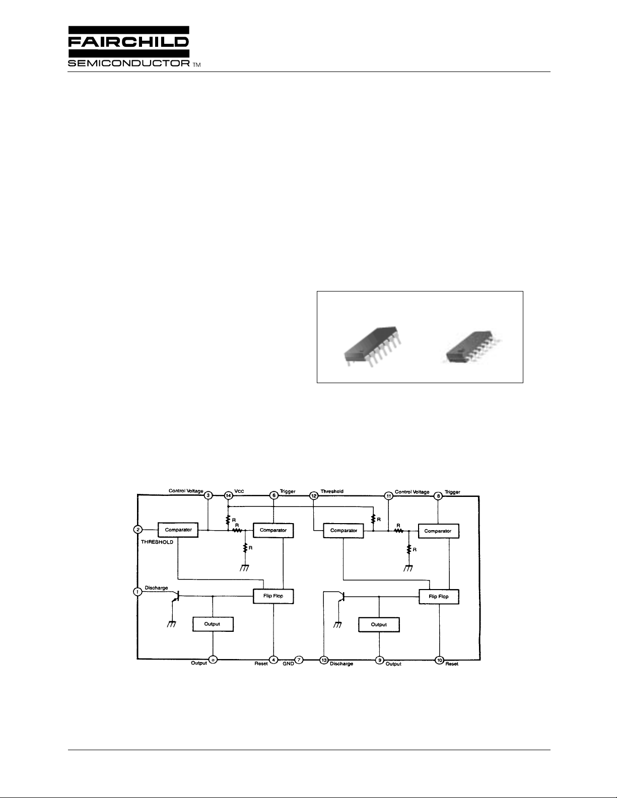
Internal Block Diagram
Description
The LM556/NE556 series dual monolithic timing circuits
are a highly stable controller capable of producing accurate
time delays or oscillation. The LM556/NE556 is a dual
LM555. Timing is provided an external resistor and capacitor for each timing function. The two timer s operate independently of each other, sharing only V
circuits may be triggered and reset on falling waveforms.
The output structures may sink or source 200mA.
14-DIP
1
14-SOP
and ground. The
CC
1
©2001 Fairchild Semiconductor Corporation
Rev. 1.0.0

LM556/NE556
Absolute Maximum Ratings (TA = 25°°°°C)
Parameter Symbol Value Unit
Supply Voltage V
Lead Temperature (soldering 10sec) T
Power Dissipation P
CC
LEAD
D
16 V
300 °C
600 mW
Operating Temperature Range
LM556/NE556
Storage Temperature Range T
T
OPR
STG
0 ~ + 70 °C
- 65 ~ + 150 °C
2

Electrical Characteristics
(TA = 25°C, VCC = 5 ~ 15V, unless otherwise specified)
Parameter Symbol Conditions Min. Typ. Max. Units
Supply Voltage V
Supply Current *
(two timers)
1
(low state)
Timing Error *
(monostable)
2
Initial Accuracy
Drift with Temperature
Drift with Supply Voltage
Control Voltage V
Threshold Voltage V
Threshold Current*
3
Trigger Voltage V
Trigger Current I
Reset Voltage*
5
Reset Current I
Low Output Voltage V
High Output Voltage V
Rise Time of Output t
Fall Time of Output t
Discharge Leakage Current I
Matching Characteristics*
4
Initial Accuracy
Drift with Temperature
Drfit with Supply Voltage
2
Timing Error (astable)*
Initial Accuracy
Drift with Temperature
Drift with Supply Voltage
CC
I
CC
ACCUR
∆t/∆T
∆t/∆V
CC
C
TH
I
TH
TR
TR
V
RST
RST
OL
OH
R
F
LKG
ACCUR
∆t/∆T
∆t/∆V
CC
ACCUR
∆t/∆T
∆t/∆Vcc
VCC = 5V, RL = ∞
V
CC
R
A
C = 0.1µF
T = 1.1RC
VCC = 15V 9.0 10.0 11.0 V
V
CC
VCC = 15V 8.8 10.0 11.2 V
V
CC
VCC = 15V 4.5 5.0 5.6 V
V
CC
V
TR
VCC = 15V
I
SINK
I
SINK
I
SINK
I
SINK
V
CC
I
SINK
I
SINK
VCC = 15V
I
I
V
CC
I
V
CC
R
A,RB
C = 0.1µF
-4.5-16V
= 15V, RL = ∞
= 2KΩ to 100KΩ
-
-
5
16
0.75
50
12
30
-
0.1
= 5V 2.6 3.33 4.0 V
= 5V 2.4 3.33 4.2 V
- - 30 250 nA
= 5V 1.1 1.6 2.2 V
= 0V - 0.01 2.0 µA
- 0.4 0.6 1.0 V
- - 0.03 0.6 mA
= 10mA
= 50mA
= 100mA
= 200mA
-
0.1
0.4
2.0
2.5
0.25
0.75
3.2
= 5V
= 8mA
= 5mA
SOURCE
SOURCE
= 5V
SOURCE
= 200mA
= 100mA 12.75
= 100mA 2.75 3.3
0.25
0.15
12.5
13.3
0.35
0.25
-V
-
- - 100 300 ns
- - 100 300 ns
- - 10 100 nA
--
= 15V
= 1KΩ to 100KΩ
1.0
10
0.2
2.25
-
150
2.0
0.5
-
0.3
LM556/NE556
mA
mA
%
ppm/°C
%/V
V
V
V
%
ppm/°C
%/V
%
ppm/°C
%/V
Notes:
*1. Supply curr ent when output is high is typically 1.0m A less at V
*2. Tested at V
*3. This will determine the maxi mum value of R
The maximum total R = 20MΩ, and for 5V operation the maximum total R = 6.6MΩ.
*4. Matching characteristics refer to the difference between performance characteristics of each timer section in the monostable
mode.
*5. As reset voltage lowers, timing is inhibited and then the output goes low.
= 5V and VCC = 15V
CC
+ RB for 15V operation.
A
CC
= 5V
3
 Loading...