

Fairchild Semiconductor NDS9430A Datasheet
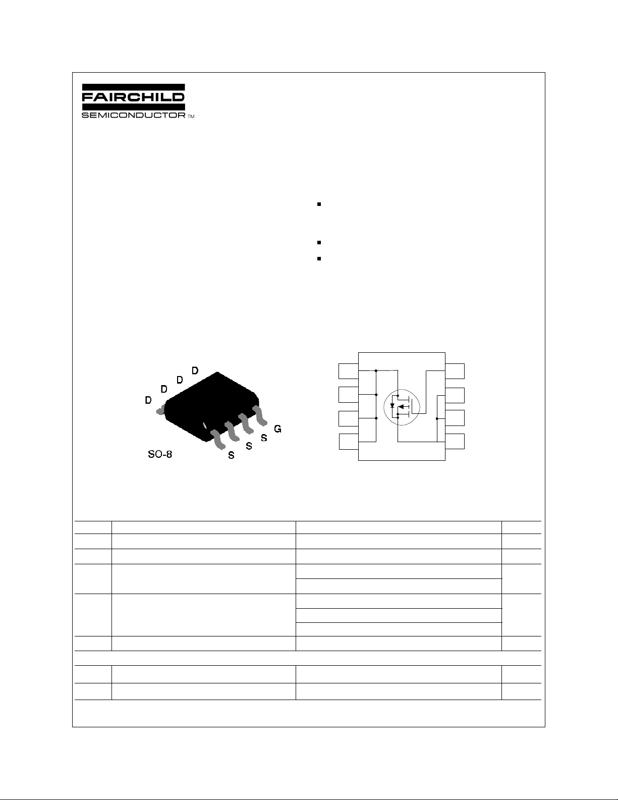
NDS9430A
Single P-Channel Enhancement Mode Field Effect Transistor
General Description Features
December 1997
These P-Channel enhancement mode power field effect
transistors are produced using National's proprietary, high cell
density, DMOS technology. This very high density process is
especially tailored to minimize on-state resistance, provide
superior switching performance, and withstand high energy
pulses in the avalanche and commutation modes. These
devices are particularly suited for low voltage applications such
-5.3A, -20V. R
R
R
High density cell design for extremely low R
= 0.05Ω @ VGS = -10V
DS(ON)
= 0.065Ω @ VGS = -6V
DS(ON)
= 0.09Ω @ VGS = -4.5V.
DS(ON)
DS(ON).
High power and current handling capability in a widely used
surface mount package.
as notebook computer power management and other battery
powered circuits where fast switching, low in-line power loss,
and resistance to transients are needed.
___________________________________________________________________________________________
5
6
7
8
4
3
2
1
Absolute Maximum Ratings T
= 25°C unless otherwise noted
A
Symbol Parameter NDS9430A Units
V
DSS
V
GSS
I
D
Drain-Source Voltage -20 V
Gate-Source Voltage ± 20 V
Drain Current - Continuous (Note 1a) ± 5.3 A
- Pulsed ± 20
P
D
TJ,T
Maximum Power Dissipation (Note 1a) 2.5 W
(Note 1b)
(Note 1c)
Operating and Storage Temperature Range -55 to 150 °C
STG
1.2
1
THERMAL CHARACTERISTICS
R
θ
R
θ
© 1997 Fairchild Semiconductor Corporation
Thermal Resistance, Junction-to-Ambient (Note 1a) 50 °C/W
JA
Thermal Resistance, Junction-to-Case (Note 1) 25 °C/W
JC
NDS9430A Rev.A
Electrical Characteristics (T
= 25°C unless otherwise noted)
A
Symbol Parameter Conditions Min Typ Max Units
OFF CHARACTERISTICS
BV
I
DSS
I
GSSF
I
GSSR
DSS
Drain-Source Breakdown Voltage VGS = 0 V, ID = -250 µA -20 V
Zero Gate Voltage Drain Current
Gate - Body Leakage, Forward
Gate - Body Leakage, Reverse
VDS = -16 V, V
VDS = -10 V, V
= 0 V
GS
= 0 V TJ = 70°C -5 µA
GS
VGS = 20 V, VDS = 0 V
VGS = -20 V, VDS= 0 V
-1 µA
100 nA
-100 nA
ON CHARACTERISTICS (Note 2)
V
R
GS(th)
DS(ON)
Gate Threshold Voltage
Static Drain-Source On-Resistance
VDS = VGS, ID = -250 µA
TJ = 125°C
VGS = -10 V, ID = -5.3 A
TJ = 125°C
-1 -1.4 -3 V
-0.7 -1 -2
0.038 0.05
0.054 0.1
Ω
VGS = -6 V, ID = -4.7 A 0.046 0.065
0.064 0.09
-3.6
I
g
D(on)
VGS = -4.5 V, ID = -4.2 A
On-State Drain Current VGS = -10 V, VDS = -5 V -15 A
VGS = -4.5, VDS = -5V
FS
Forward Transconductance VDS = 15 V, ID = 5.3 A 10 S
DYNAMIC CHARACTERISTICS
C
iss
C
oss
C
rss
Input Capacitance
Output Capacitance 610 pF
VDS = 15 V, V
f = 1.0 MHz
GS
= 0 V,
Reverse Transfer Capacitance 220 pF
950 pF
SWITCHING CHARACTERISTICS (Note 2)
t
t
t
t
Q
Q
Q
D(on)
r
D(off)
f
Turn - On Delay Time
Turn - On Rise Time 18 60 ns
VDD = -10 V, ID = -1 A,
V
= -10 V, R
GEN
GEN
= 6 Ω
Turn - Off Delay Time 80 120 ns
Turn - Off Fall Time 45 100 ns
g
gs
gd
Total Gate Charge
Gate-Source Charge 3 nC
Gate-Drain Charge 9 nC
VDS = -10 V,
ID = -5.3 A, VGS = -10 V
10 30 ns
29 50 nC
NDS9430A Rev.A
Electrical Characteristics (T
= 25°C unless otherwise noted)
A
Symbol Parameter Conditions Min Typ Max Units
DRAIN-SOURCE DIODE CHARACTERISTICS AND MAXIMUM RATINGS
I
S
V
SD
t
rr
Notes:
1. R
design while R
P
Typical R
Maximum Continuous Drain-Source Diode Forward Current -2.1 A
Drain-Source Diode Forward Voltage
Reverse Recovery Time
is the sum of the junction-to-case and case-to-ambient thermal resistance where the case thermal reference is defined as the solder mounting surface of the drain pins. R
JA
θ
(t)
D
is determined by the user's board design.
CA
θ
T
=
R
JA
θ
a. 50oC/W when mounted on a 1 in2 pad of 2oz cpper.
b. 105oC/W when mounted on a 0.04 in2 pad of 2oz cpper.
c. 125oC/W when mounted on a 0.006 in2 pad of 2oz cpper.
T
J−TA
=
(t)
R
θJ A
θ
J C
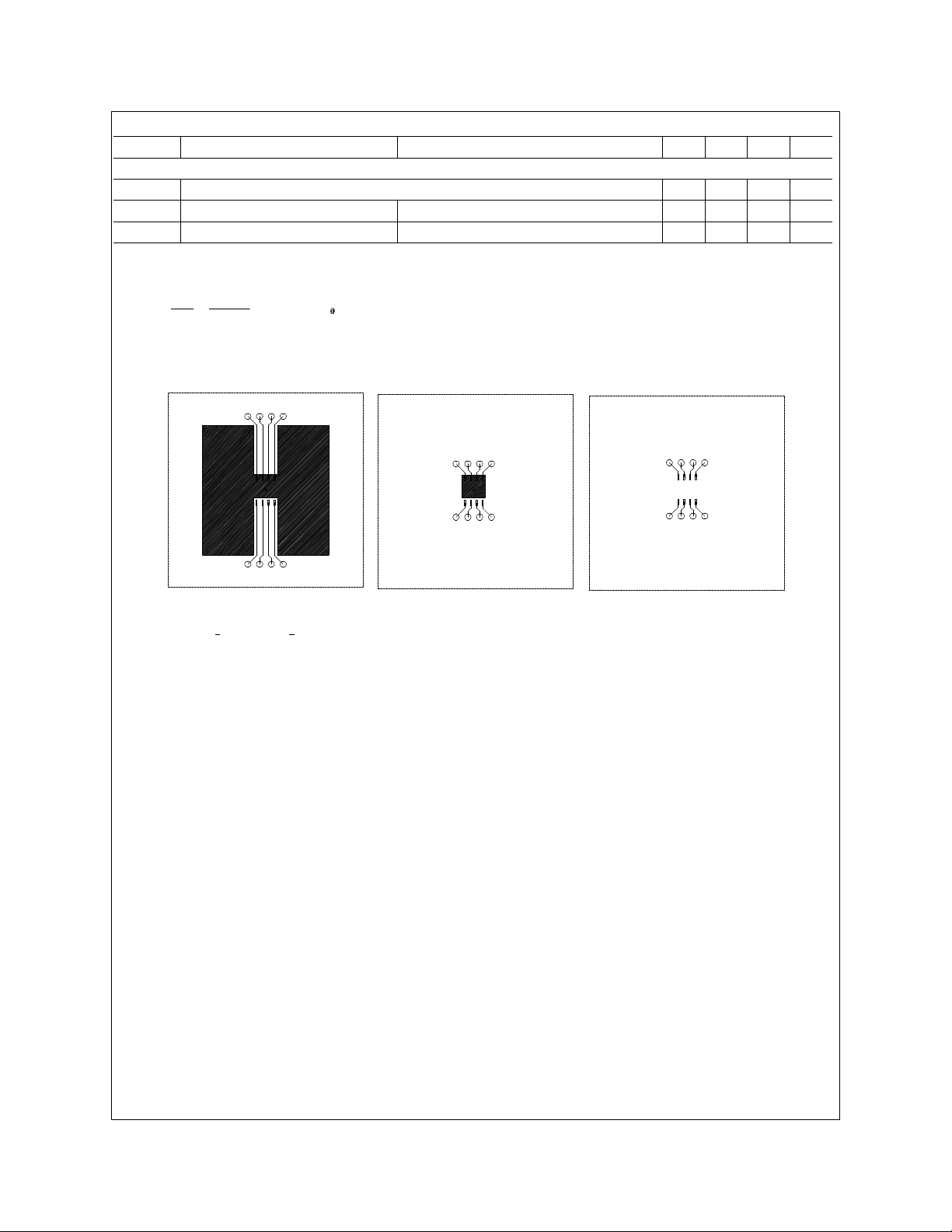
using the board layouts shown below on 4.5"x5" FR-4 PCB in a still air environment:
J−TA
+R
2
= I
(t) × R
DS(O N ) T
D
(t)
θ
CA
J
1a
VGS = 0 V, IS = -2.4 A
(Note 2)
VGS = 0V, IF = -2.4 A, dIF/dt = 100 A/µs
1b
1c
-0.85 -1.2 V
100 ns
is guaranteed by
JC
θ
Scale 1 : 1 on letter size paper
2. Pulse Test: Pulse Width < 300µs, Duty Cycle < 2.0%.
NDS9430A Rev.A
 Loading...