

Fairchild Semiconductor NDP608A Datasheet
May 1994
NDP608A / NDP608AE / NDP608B / NDP608BE
NDB608A / NDB608AE / NDB608B / NDB608BE
N-Channel Enhancement Mode Field Effect Transistor
General Description Features
These N-channel enhancement mode power field
effect transistors are produced using Fairchild's
proprietary, high cell density, DMOS technology. This
very high density process has been especially
tailored to minimize on-state resistance, provide
superior switching performance, and withstand high
energy pulses in the avalanche and commutation
modes. These devices are particularly suited for low
voltage applications such as automotive, DC/DC
converters, PWM motor controls, and other battery
powered circuits where fast switching, low in-line
power loss, and resistance to transients are needed.
_____________________________________________________________________
36 and 32A, 80V. R
= 0.042and 0.045Ω.
DS(ON)
Critical DC electrical parameters specified at
elevated temperature.
Rugged internal source-drain diode can eliminate
the need for an external Zener diode transient
suppressor.
175°C maximum junction temperature rating.
High density cell design (3 million/in²) for extremely
low R
DS(ON)
.
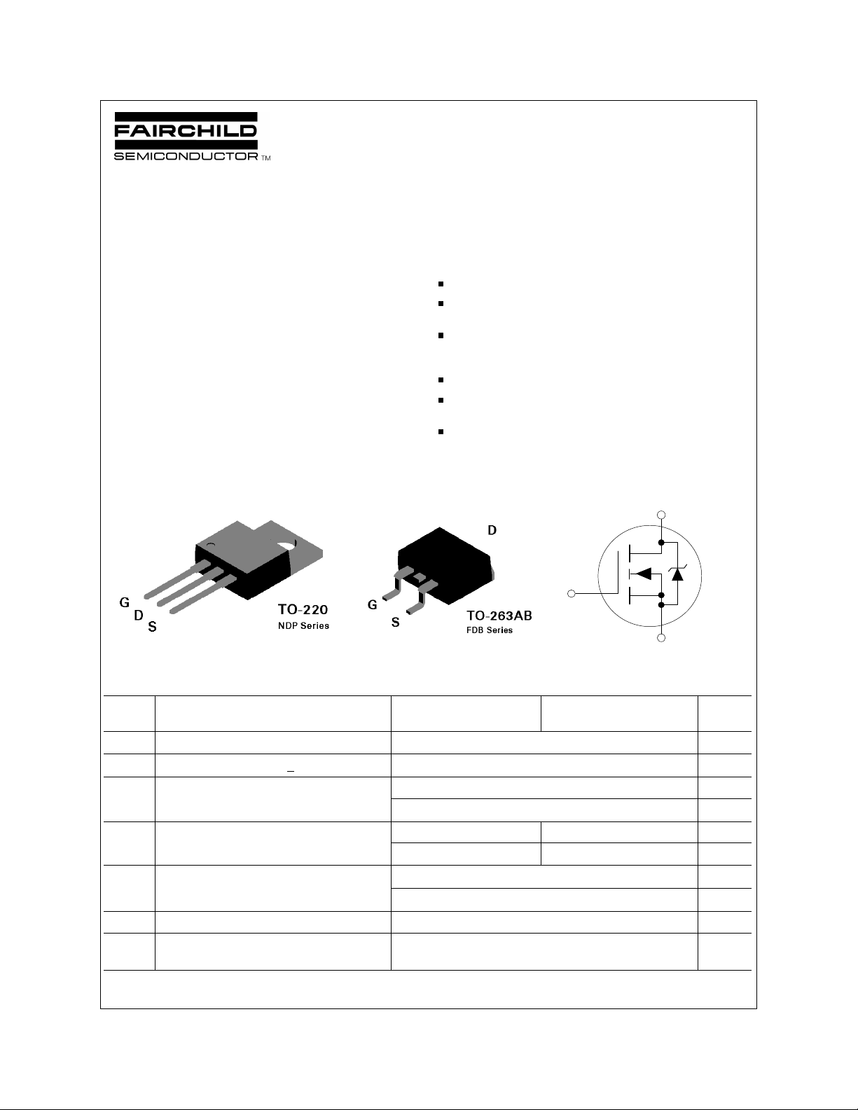
TO-220 and TO-263 (D2PAK) package for both
through hole and surface mount applications.
D
Absolute Maximum Ratings T
Symbol Parameter
V
V
V
I
P
TJ,T
T
DSS
DGR
GSS
D
D
L
Drain-Source Voltage 80 V
Drain-Gate Voltage (RGS < 1 MΩ)
Gate-Source Voltage - Continuous ±20 V
- Nonrepetitive (tP < 50 µs)
Drain Current - Continuous 36 32 A
- Pulsed 144 128 A
Total Power Dissipation @ TC = 25°C
Derate above 25°C
Operating and Storage Temperature Range -65 to 175 °C
STG
Maximum lead temperature for soldering
purposes, 1/8" from case for 5 seconds
= 25°C unless otherwise noted
C
NDP608A NDP608AE
NDB608A NDB608AE
G
S
NDP608B NDP608BE
NDB608B NDB608BE Units
80 V
±40 V
100 W
0.67
W/°C
275 °C
© 1997 Fairchild Semiconductor Corporation
NDP608.SAM
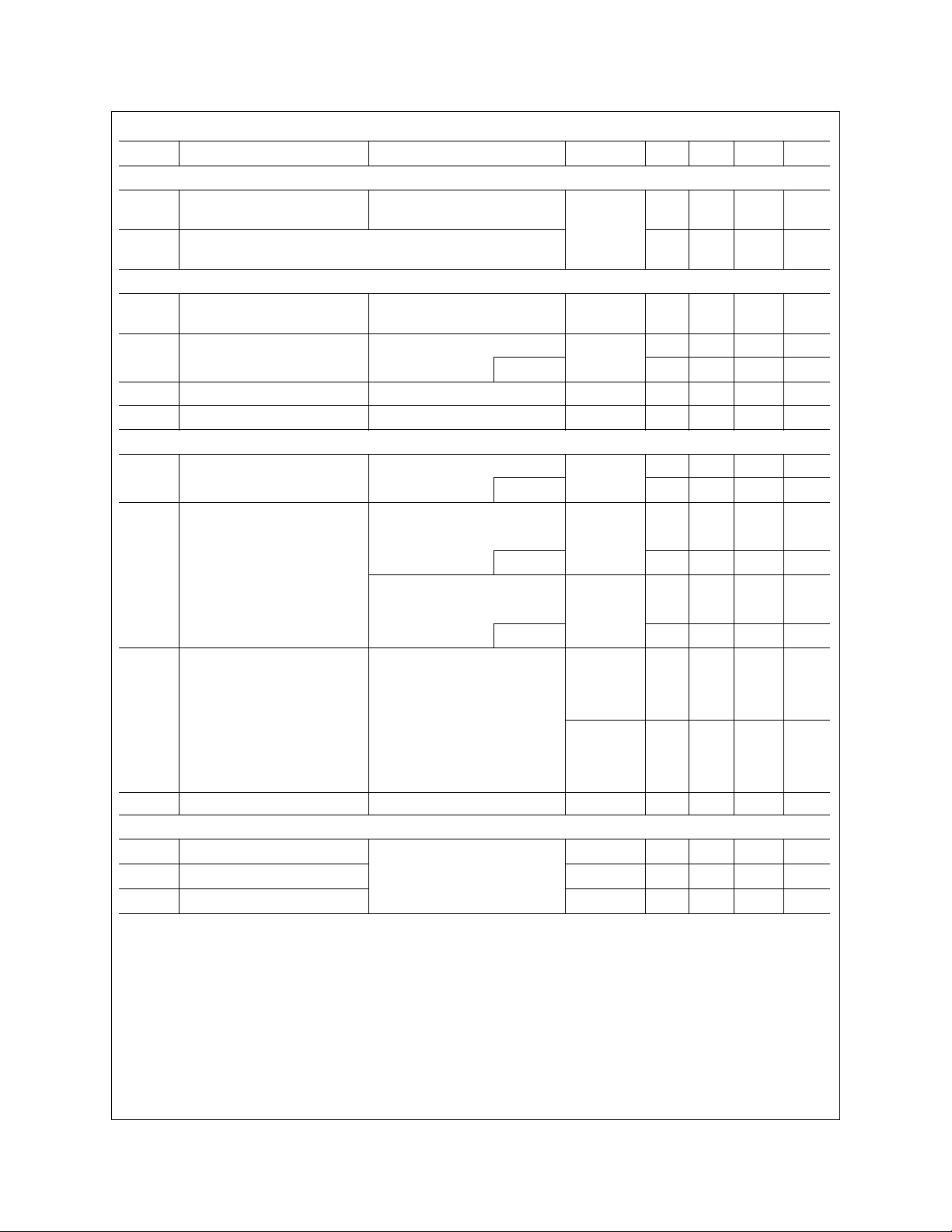
Electrical Characteristics (T
= 25°C unless otherwise noted)
C
Symbol Parameter Conditions Type Min Typ Max Units
DRAIN-SOURCE AVALANCHE RATINGS (Note 1)
E
AS
I
AR
Single Pulse Drain-Source
Avalanche Energy
Maximum Drain-Source Avalanche Current 36 A
VDD = 25 V, ID = 36 A NDP608AE
NDP608BE
NDB608AE
NDB608BE
200 mJ
OFF CHARACTERISTICS
BV
Drain-Source Breakdown
DSS
VGS = 0 V, ID = 250 µA ALL 80 V
Voltage
I
DSS
I
GSSF
I
GSSR
Zero Gate Voltage Drain
Current
VDS = 80 V,
V
= 0 V
GS
TJ = 125°C
ALL 250 µA
1 mA
Gate - Body Leakage, Forward VGS = 20 V, VDS = 0 V ALL 100 nA
Gate - Body Leakage, Reverse
VGS = -20 V, VDS = 0 V
ALL -100 nA
ON CHARACTERISTICS (Note 2)
V
R
GS(th)
DS(ON)
Gate Threshold Voltage
Static Drain-Source
On-Resistance
VDS = VGS,
ID = 250 µA
VGS = 10 V,
ID = 18 A
TJ = 125°C
ALL 2 2.9 4 V
1.4 2.3 3.2 V
NDP608A
0.031 0.042
NDP608AE
NDB608A
0.05 0.08
0.045
VGS = 10 V,
ID = 16 A
TJ = 125°C
NDB608AE
NDP608B
NDP608BE
NDB608B
0.09
I
D(on)
TJ = 125°C
NDB608BE
On-State Drain Current VGS = 10 V, VDS = 10 V NDP608A
36 A
NDP608AE
NDB608A
NDB608AE
NDP608B
32 A
NDP608BE
NDB608B
NDB608BE
g
FS
Forward Transconductance VDS = 10 V, ID = 18 A ALL 10 17.5 S
DYNAMIC CHARACTERISTICS
C
iss
C
oss
C
rss
Input Capacitance VDS = 25 V, VGS = 0 V,
Output Capacitance ALL 390 500 pF
f = 1.0 MHz
Reverse Transfer Capacitance ALL 140 200 pF
ALL 1370 1800 pF
Ω
Ω
Ω
Ω
NDP608.SAM
 Loading...