

Fairchild Semiconductor NC7SP58, NC7SP57 Datasheet

NC7SP57 • NC7SP58
NC7SP57 • NC7SP58 TinyLogic
October 2001
Revised March 2003
TinyLogic
ULP Universal Configurable
2-Input Logic Gates
General Description
The NC7SP57 and the NC7SP58 are Universal Configurable 2-Input Logic Gates from Fairchild’s Ultra Low
Power (ULP) Serie s of TinyLogic
where battery life is critical, this product is designed for
ultra low power consumption within the V
range of 0. 9V t o 3 . 6V. Ea c h d ev ic e is c ap a ble of be in g c on figured for 1 of 5 unique 2-inpu t logic f uncti ons. Any po ssible 2-input combinatorial logic function can be
implemented as shown in the Function Selection Table.
Device functionality is selected by how the device is wired
at the board level. Figure 1 through Figure 10 illustrate how
to connect the NC7S P57 and NC7SP58 respectively for
the desired logic function. All inputs have been implemented with hysteresis.
The internal circ uit is composed o f a minimum of inverter
stages including the output buffer, to enable ultra low
dynamic power.
The NC7SP57 and NC7SP58, for lower drive requirements, are uniquely designed for optimized power and
speed, and are fabricated wit h an advanced CMOS technology to achieve best in class ope rat ion w hile mai n tain i ng
extremely low CMOS power dissipation.
. Ideal for applicat ions
operating
CC
Features
■ 0.9V to 3.6V VCC supply operation
■ 3.6V overvoltage tolerant I/O’s at V
■ t
PD
5 ns typ for 3.0V to 3.6V V
6 ns typ for 2.3V to 2.7V V
8 ns typ for 1.65V to 1.95V V
10 ns typ for 1.40V to 1.60V V
14 ns typ for 1.10V to 1.30V V
40 ns typ for 0.90V V
■ Power-Off high impedance inputs and outputs
■ Static Drive (I
±2.6 mA @ 3.00V V
±2.1 mA @ 2.30V V
±1.5 mA @ 1.65V V
±1.0 mA @ 1.40V V
±0.5 mA @ 1.10V V
±20 µA@ 0.9V V
■ Uses patented Quiet Series noise/EMI reduction
circuitry
■ Ultra small MicroPak
■ Ultra low dynamic power
OH/IOL
CC
CC
CC
)
CC
CC
CC
CC
CC
CC
leadfree package
CC
CC
CC
CC
from 0.9V to 3.6V
ULP Universal Configurable 2-Input Logic Gates
Ordering Code:
Order Number
NC7SP57P6X MAA06A P57 6-Lead SC70, EIAJ SC88, 1.25mm Wide 3k Units on Tape and Reel
NC7SP57L6X MAC06A K9 6-Lead MicroPak, 1.0mm Wide 5k Units on Tape and Reel
NC7SP58P6X MAA06A P58 6-Lead SC70, EIAJ SC88, 1.25mm Wide 3k Units on Tape and Reel
NC7SP58L6X MAC06A L3 6-Lead MicroPak, 1.0mm Wide 5k Units on Tape and Reel
TinyLogic is a registered tradema rk of F airc hild Semiconduct or Corporation.
Quiet Series and MicroPak are trademarks of Fairchild Semiconductor Corporation.
© 2003 Fairchild Semiconductor Corporation DS500701 www.fairchildsemi.com
Package Product Code
Number Top Mark
Package Description Supplied As
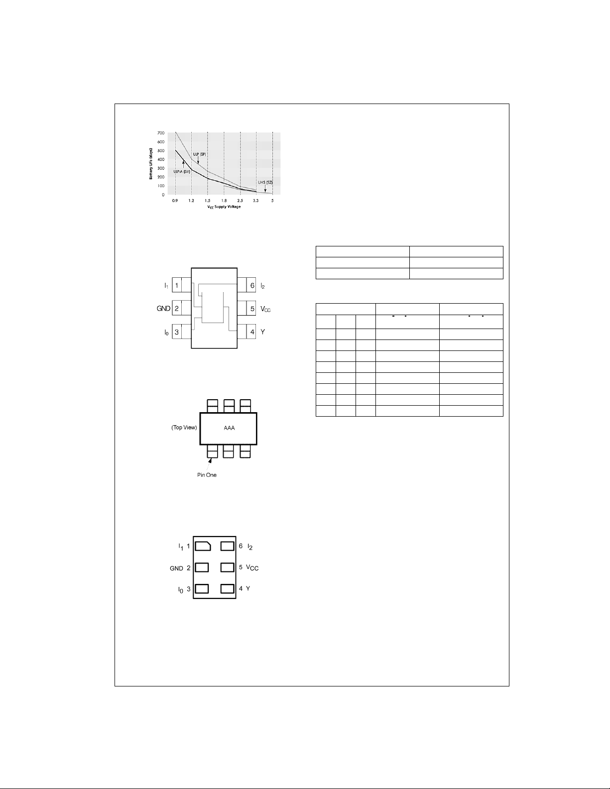
Battery Life vs. VCC Supply Voltage
NC7SP57 • NC7SP58
TinyLogic ULP and ULP-A with up to 50% less power consumption can
extend your battery life significantly.
Battery Life = (V
Where, P
Assumes ideal 3.6 V L ithiu m Ion ba ttery wit h cu rrent rati ng of 900m AH and
derated 90% and dev ic e frequency at 10MH z , with C
device
battery
= (I
*I
*.9)/(P
battery
* VCC) + (CPD + CL)* V
CC
device
)/24hrs/day
2
* f
CC
= 15 pF load
L
Connection Diagrams
Pin Assignments for SC70
(Top View)
NC7SP57 and NC7SP58
Pin One Orientation Diagram
AAA = Product Code Top Mark - see ordering code
Note: Orientation of Top Mark determines Pin One lo cation. R ead the top
product code mark left to right, Pin One is the lower left pin (see diagram).
Pad Assignments for MicroPak
Pin Descriptions
Pin Name Description
I
, I1, I
0
2
Data Input
YOutput
Function Table
Input NC7SP57 NC7SP58
I
2I1I0
LLL H L
LLH L H
LHL H L
LHH L H
HLL L H
HLH L H
HHL H L
HHH H L
H = HIGH Logic Level L = LOW Logic Level
Y = (I0)•(I2)+(I1)•(I2)Y = (I0)•(I2)+(I1)•(I2)
(Top Thru View)
www.fairchildsemi.com 2
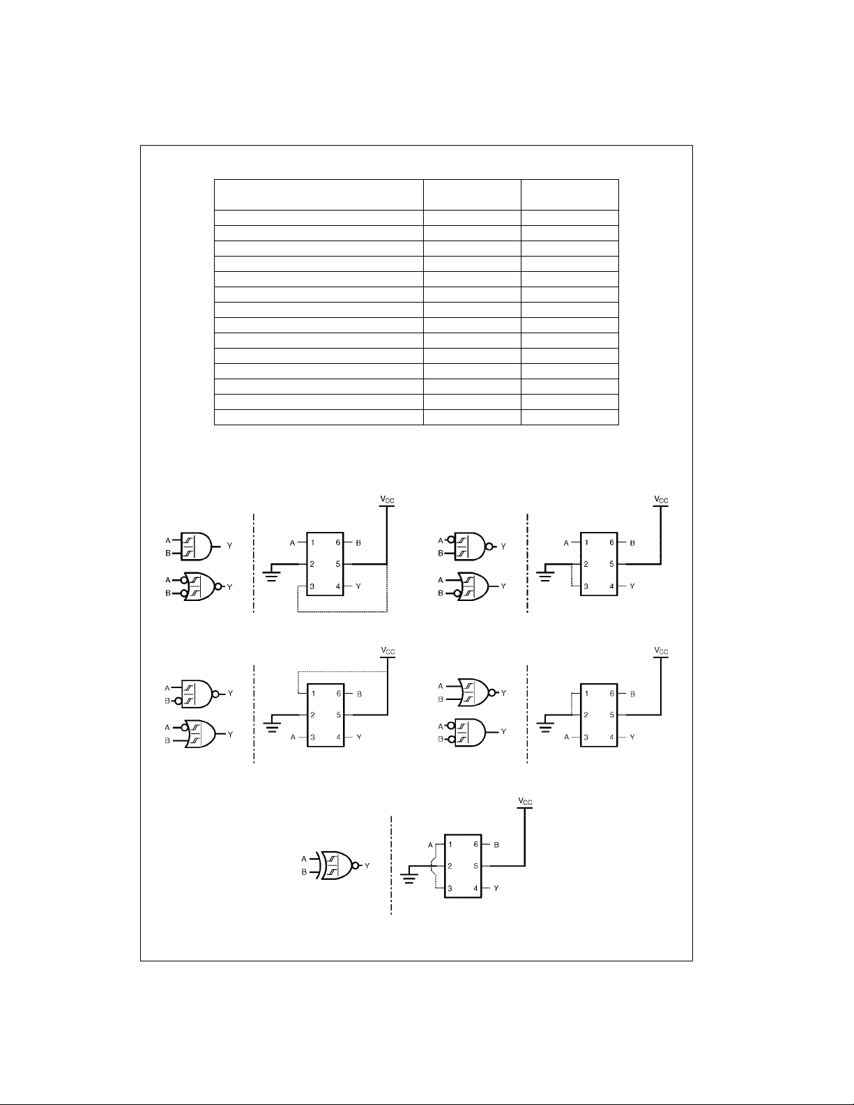
Function Selection Table
2-Input Logic Function
2-Input AND NC7SP57 Figure 1
2-Input AND with inverted input NC7SP58 Figures 7, 8
2-Input AND with both inputs inverted NC7SP57 Figure 4
2-Input NAND NC7SP58 Figure 6
2-Input NAND with inverted input NC7SP57 Figures 2, 3
2-Input NAND with both inputs inverted NC7SP58 Figure 9
2-Input OR NC7SP58 Figure 9
2-Input OR with inverted input NC7SP57 Figures 2, 3
2-Input OR with both inputs inverted NC7SP58 Figure 6
2-Input NOR NC7SP57 Figure 4
2-Input NOR with inverted input NC7SP58 Figures 7, 8
2-Input NOR with both inputs inverted NC7SP57 Figure 1
2-Input XOR NC7SP58 Figure 10
2-Input XNOR NC7SP57 Figure 5
Device Connection
Selection Configuration
Logic Configurations NC7SP57
Figure 1 through Figure 5 show the logical functions that can be implemented using the NC7SP57. The diagrams show the
DeMorgan’s equivalent logic duals for a given 2-input function. Next to the logical implementation is the board level physical
implementation of how the pins of the function should be connected.
NC7SP57 • NC7SP58
FIGURE 1. 2-Input AND Gate FIGURE 2. 2-Input NAND with Inverted A Input
FIGURE 3. 2-Input NAND with Inverted B Input FIGURE 4. 2-Input NOR Gate
FIGURE 5. 2-Input XNOR Gate
3 www.fairchildsemi.com
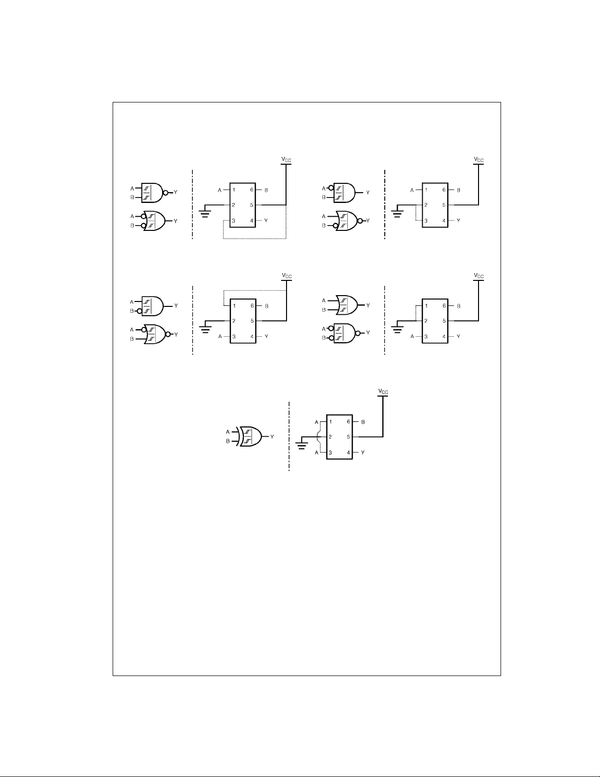
Logic Configurations NC7SP58
Figure 6 throu gh Figure 10 s how the lo gical fun ctions th at can b e implemen ted us ing the NC 7SP58. The diag rams sho w
the DeMorgan’s equiva lent logic duals for a given 2- input function. Next to the logical implementation is th e board level
physical implementation of how the pins of the function should be connected.
NC7SP57 • NC7SP58
FIGURE 6. 2-Input NAND Gate FIGURE 7. 2-Input AND with Inverted A Input
FIGURE 8. 2-Input AND with Inverted B Input FIGURE 9. 2-Input OR Gate
FIGURE 10. 2-Input XOR Gate
www.fairchildsemi.com 4
 Loading...