

Fairchild Semiconductor NC7SP04 Datasheet
NC7SP04
NC7SP04 TinyLogic
October 2001
Revised February 2003
TinyLogic
ULP Inverter
General Description
The NC7SP04 is a single inverter from Fairchild’s Ultra
Low Power (ULP) Series of TinyLogic
tions where battery life i s critical, this product is de signed
for ultra low power consumpt ion within the V
range of 0.9V to 3.6V.
The internal circ uit is composed o f a minimum of inverter
stages including the output buffer, to enable ultra low static
and dynamic power.
The NC7SP04, for lower drive requirements, is uniq uely
designed for optimi zed po wer and speed, and is fab ri cat ed
with an advanced CMOS technology to achieve best in
class speed operation while maintaining extremely low
CMOS power dissipation.
. Ideal for app lica-
operating
CC
Features
■ 0.9V to 3.6V VCC supply operation
■ 3.6V overvoltage tolerant I/O’s at V
■ t
PD
4.0 ns typ for 3.0V to 3.6V V
5.0 ns typ for 2.3V to 2.7V V
6.0 ns typ for 1.65V to 1.95V V
7.0 ns typ for 1.40V to 1.60V V
11.0 ns typ for 1.10V to 1.30V V
27.0 ns typ for 0.90V V
CC
■ Power-Off high impedance inputs and outputs
■ Static Drive (I
±2.6 mA @ 3.00V V
±2.1 mA @ 2.30V V
±1.5 mA @ 1.65V V
±1.0 mA @ 1.40V V
±0.5 mA @ 1.10V V
±20 µA@ 0.9V V
OH/IOL
)
CC
CC
CC
CC
CC
CC
■ Uses patented Quiet Series noise/EMI reduction
circuitry
■ Ultra small MicroPak
leadfree package
■ Ultra low dynamic power
CC
CC
CC
CC
CC
from 0.9V to 3.6V
CC
ULP Inverter
Ordering Code:
Order Number
NC7SP04P5X MAA05A P04 5-Lead SC70, EIAJ SC-88a, 1.25mm Wide 3k Units on Tape and Reel
NC7SP04L6X MAC06A J6 6-Lead MicroPak, 1.0mm Wide 5k Units on Tape and Reel
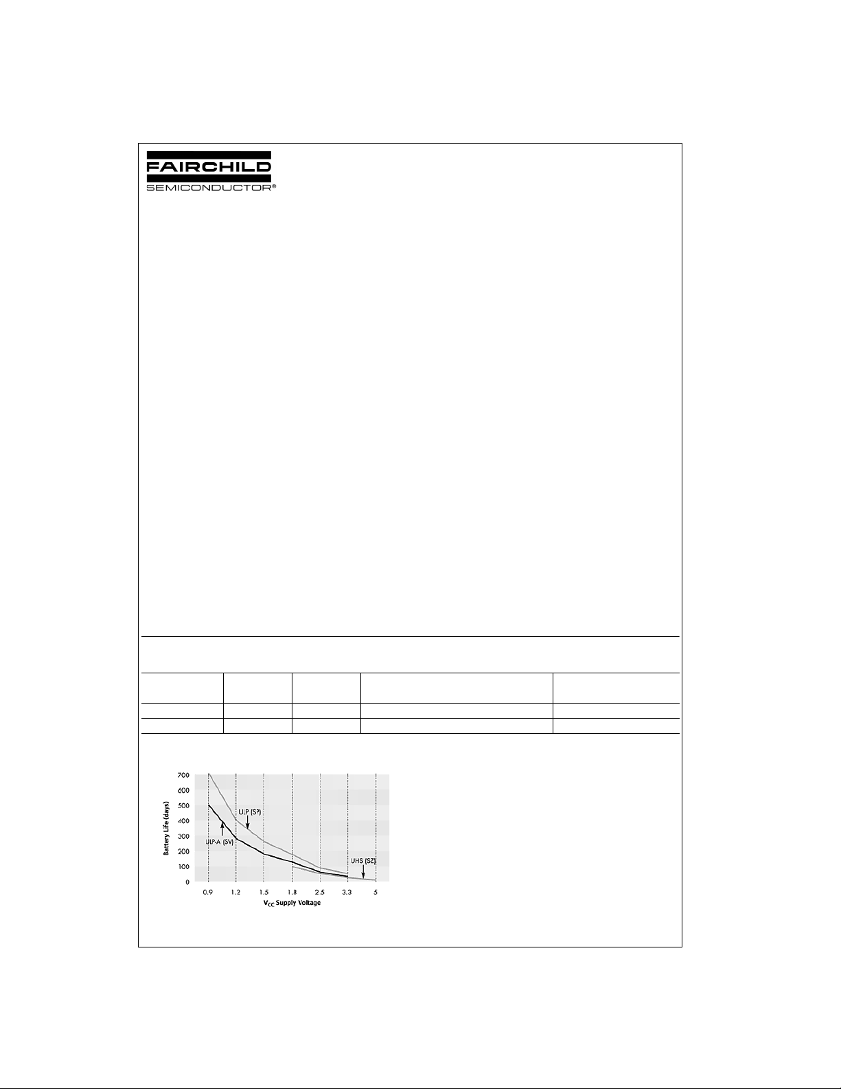
Battery Life vs. V
TinyLogic is a registered trademark, and Quiet Series and MicroPak are trademarks of Fairchild Semiconductor Corporation.
© 2003 Fairchild Semiconductor Corporation DS500597 www.fairchildsemi.com
Package Product Code
Number Top Mark
Supply Voltage
CC
Package Description Supplied As
TinyLogic ULP and ULP -A with up to 50% les s power consumption can
extend your battery lif e significantly.
Battery Life = (V
Where, P
device
Assumes ideal 3.6V Lithium Ion battery with current rating of 900mAH and
derated 90% and device frequency at 10MHz, with C
= (I
battery
*I
* VCC) + (C
CC
battery
*.9) / (P
PD
device
+ CL) * V
) / 24hrs/day
2
* f
CC
= 15 pF load
L
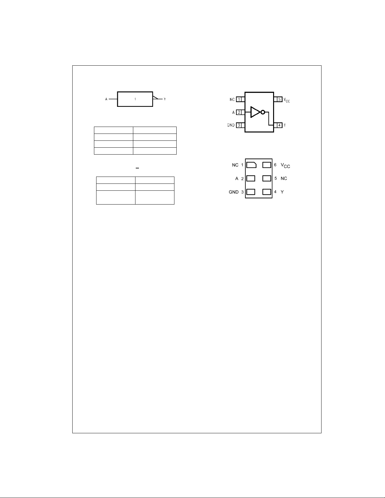
Logic Symbol
Connection Diagrams
NC7SP04
Pin Descriptions
Pin Names Description
NC No Connect
Function Table
Inputs Output
H = HIGH Logic Level
L = LOW Logic Level
IEEE/IEC
A Input
Y Output
Y = A
AY
LH
HL
Pin Assignments for SC70
(Top View)
Pad Assignments for MicroPak
(Top Thru View)
www.fairchildsemi.com 2
Absolute Maximum Ratings(Note 1) Recommended Operating
Supply Voltage (VCC) −0.5V to +4.6V
DC Input Voltage (V
DC Output Voltage (V
HIGH or LOW State (Note 2)
V
= 0V −0.5V to 4.6V
CC
DC Input Diode Current (I
DC Output Diode Current (I
V
< 0V −50 mA
OUT
V
> V
OUT
CC
DC Output Source/Sink Current (I
DC V
or Ground Current per
CC
Supply Pin (I
Storage Temperature Range (T
) −0.5V to +4.6V
IN
)
OUT
) VIN < 0V ±50 mA
IK
)
OK
or Ground) ± 50 mA
CC
STG
−0.5V to V
) ± 50 mA
OH/IOL
CC
) −65°C to +150°C
+0.5V
+50 mA
Conditions
Supply Voltage 0.9V to 3.6V
Input Voltage (V
Output Voltage (V
HIGH or LOW State 0V to V
VCC = 0V 0V to 3.6V
Output Current in I
VCC = 3.0V to 3.6V ±2.6 mA
V
= 2.3V to 2.7V ± 2.1 mA
CC
V
= 1.65V to 1.95V ± 1.5 mA
CC
= 1.40V to 1.60V ± 1 mA
V
CC
V
= 1.10V to 1.30V ±0.5 mA
CC
V
= 0.9V ±20 µA
CC
Free Air Operating Temperature (T
Minimum Input Edge Rate (
V
= 0.8V to 2.0V, VCC = 3.0V 10 ns/V
IN
Note 1: Absolute Maximum Ratings: are those values beyond which the
safety of the device can not be gu arant eed. The de vice sh ould no t be operated at these limits. The parametric values defined in the Electrical Characteristics tables are not guaranteed at the absolute maximum ratings. The
“Recommended Operating Con ditions” table will define the conditions for
actual device opera tion.
Absolute Maximum Rating must be observed.
Note 2: I
O
Note 3: Unused inputs must be held HIGH or LOW. They may not float.
(Note 3)
) 0V to 3.6V
IN
)
OUT
OH/IOL
) −40°C to +85°C
A
∆t/∆V)
DC Electrical Characteristics
V
Symbol Parameter
V
HIGH Level 0.90 0.65 x V
IH
Input Voltage 1.10 ≤ VCC ≤ 1.30 0.65 x V
V
LOW Level 0.90 0.35 x V
IL
Input Voltage 1.10 ≤ V
V
HIGH Level 0.90 V
OH
Output Voltage 1.10 ≤ VCC ≤ 1.30 VCC − 0.1 VCC − 0.1
CC
(V) Min Max Min Max
1.40 ≤ VCC ≤ 1.60 0.65 x V
1.65 ≤ VCC ≤ 1.95 0.65 x V
2.30 ≤ VCC ≤ 2.70 1.6 1.6
≤ 3.60 2.1 2.1
3.00 ≤ V
CC
≤ 1.30 0.35 x V
CC
1.40 ≤ VCC ≤ 1.60 0.35 x V
1.65 ≤ VCC ≤ 1.95 0.35 x V
2.30 ≤ VCC ≤ 2.70 0.7 0.7
3.00 ≤ VCC ≤ 3.60 0.9 0.9
1.40 ≤ VCC ≤ 1.60 VCC − 0.1 VCC − 0.1
1.65 ≤ VCC ≤ 1.95 VCC − 0.1 VCC − 0.1
2.30 ≤ VCC ≤ 2.70 VCC − 0.1 VCC − 0.1
3.00 ≤ VCC ≤ 3.60 VCC − 0.1 VCC − 0.1
1.10 ≤ VCC ≤ 1.30 0.75 x V
1.40 ≤ VCC ≤ 1.60 1.07 0.99 IOH = −1 mA
1.65 ≤ VCC ≤ 1.95 1.24 1.22 IOH = −1.5 mA
2.30 ≤ VCC ≤ 2.70 1.95 1.87 IOH = −2.1 mA
3.00 ≤ VCC ≤ 3.60 2.61 2.55 IOH = −2.6 mA
TA = +25°CT
CC
CC
CC
CC
− 0.1 VCC − 0.1
CC
CC
0.65 x V
0.65 x V
0.65 x V
0.65 x V
CC
CC
CC
CC
0.70 x V
= −40°C to +85°C
A
CC
CC
CC
CC
0.35 x V
0.35 x V
0.35 x V
0.35 x V
CC
Units Conditions
V
CC
CC
CC
V
CC
V
NC7SP04
CC
IOH = −20 µA
IOH = −0.5 mA
3 www.fairchildsemi.com
 Loading...