


June 2002
Revised April 2003
MSX532
532 Port Digital Crosspoint Switch with LVTTL I/O’s
MSX532 532 Port Digital Crosspoint Switch with LVTTL I/O’s
General Description
The MSX family of SRAM-based bit-oriented switching
devices offer flow-through NRZ data rates of up to 150Mb/s
and registered clo ck frequencies of up to 75MHz. Th e I/O
buffers are individually configurable. The I/O buffers can be
connected to each othe r through the switch matrix, which
supports One-to-One and One-to-Many connections.
The proprietary Ra pidConfigure
fast configuration of both the I/O buffers and switch mat rix.
It also allows readback of the device for test and verification purposes. The MSX devices also support the industry
standard JTAG (IEEE 1149.1) interface for boundary scan
testing. The JTAG interface can also be used t o downlo ad
configuration data to the device. A functional block diagram
of the MSX architecture is shown in Figure 1.
parallel interface allows
Features
■ SRAM-based, in-system programmable
■ Configurable I/O Ports
• Individually programmable as input, output,
bi-directional, or Bus Repeater
• Control Signals per I/O por t: 2 input enables, 2 output
enables, 2 Global Clock inputs and Next Neighbor
Clock option
• Output data inversion: capable of inverting output
signals in flow through mode
■ Non-blocking switch matrix
• One-to-One and One-to-Many connections
Double-buffered configuration RAM cells for
simultaneous global updates
■ Registered and flow-through data modes
• Up to 75 MHz clock frequency in registered mode
• Up to 150 Mb/s in flow-through mode
■ 20 ns propagation delay in flow-through mode
■ 8 mA output current
■ Dedicated RapidConfigure parallel interface or JTAG
serial interface avail able for configur ation and r eadback
of MSX devices
■ 3.3V operation, LVTTL I/O's (5V tolerant)
■ MSX532 is offered in a 792 TBGA package
mode
Applications
• Telecom and dataco m sw itching
• Video switches and servers
• Test equipm ent
Ordering Code:
Order Number Package Number Package Description
MSX532TB792 BGA792A 792-Ball Thermally-Enhanced Ball Grid Array (TBGA), JEDEC MO-149, 1.0mm pitch,
MSX, Bus Repeater, and RapidConfigure are trademarks of Fairchild Semiconductor Corporation.
© 2003 Fairchild Semiconductor Corporation DS500746 www.fairchildsemi.com
40mm Square

MSX532
FIGURE 1. MSX 532 Functional Block Diagram
Introduction
Switch Matrix
The MSX family are SRAM-based, bit-oriented switching
devices. The main functional block of the device is a Switch
Matrix as shown in Figure 1. The Switch Matrix is an x-y
routing structur e (or grid). Each horizontal signa l trace is
hardwired to a corresponding vertical signal trace as
shown by the junction dots. An I/O Port pin connects to this
horizontal-vertical trace pair through a programmable
buffer. Signal paths through the Sw itch Matr ix ar e well ba lanced, resulting in predictable and uniform pin-to-pin
delays.
The two SRAM c ells (shown in Figure 2) are a rranged so
that a double buffered scheme can be employed. The
Active SRAM cells are responsible for establishing connections in the switch mat rix by turning ON a pass tra nsistor,
while the Loadin g SRAM cell can be used to stor e a second configuration that can be transferred to the Active
SRAM cell at any time. If the UPDATE signal is asserted
HIGH, the contents o f the Loading SRAM cell ar e transferred to the Active SRAM cell an d the switch matrix connection is either made or broken.
The UPDATE signal can be used to control when the
switch matrix is re configured. Fo r instance, a s long as the
UPDATE signal is de-asserted (held LOW), the Loading
SRAM cells for the e ntire switch matr ix could be changed
www.fairchildsemi.com 2
without affecting the current configuration of the switch.
When the UPDATE signal is asserted HIGH, the entire
switch matrix would be reconfigured simultaneously. If the
UPDATE signal is asserted continuously, all crosspoint programming commands (generated by JTAG or RapidConfigure programming cycles) will take effect immediately, since
the Loading SRAM cell’s contents will be transferred
directly to the Active SRAM cell.
FIGURE 2. MSX Switch Matrix Diagram

Introduction (Continued)
Input and Output Buffers (I/O buffers)
Each signal in the switch matrix is connected to a programmable I/O buffer, which is independently configured
through either the Ra pidConfigure o r JTAG Interface. The
I/O buffer attributes inc lude its signa l direction (input, output or bi-directional) and data flow mode (flow-th rough or
registered). The signa l can also be invert ed at the output.
Trickle current source (normally 15
µA) on the pin side and
V
DD
{
IE
CLK
{
Sources
Next
Neighbor
CLK_IN
MSX532
array side for each I/ O Port and contr ol pin is used t o pull
unused or non-driven circuits to a stable HIGH level. Figure
3 shows a basic block diagram of an I/O buffer with the
sources for the three control signals (IE, OE an d CLK ). For
any given port num ber, these three control sig nals can be
selected from one of two sour ces. The control signals are
explained in more detail in the following section.
IN
I/O
Port
CLK
Sources
Next
Neighbor
OE
CLK_OUT
{
{
V
SS
FIGURE 3. MSX I/O Buffer Block Diagram
I/O Port Function Mode
The following legend describes the various modes of the
Input or Output Ports and the specification used by the
Fairchild Development System Software for bitstream generation.
Legend:
Ax
= Switch Matrix Signal
Px
= I/O Po rt Signa l
= Input Enable
IE
OE
= Output Enable (Active LOW)
CLK
= Clock
OUT
Switch
Matrix
BR
Next-Neighbor Clocking
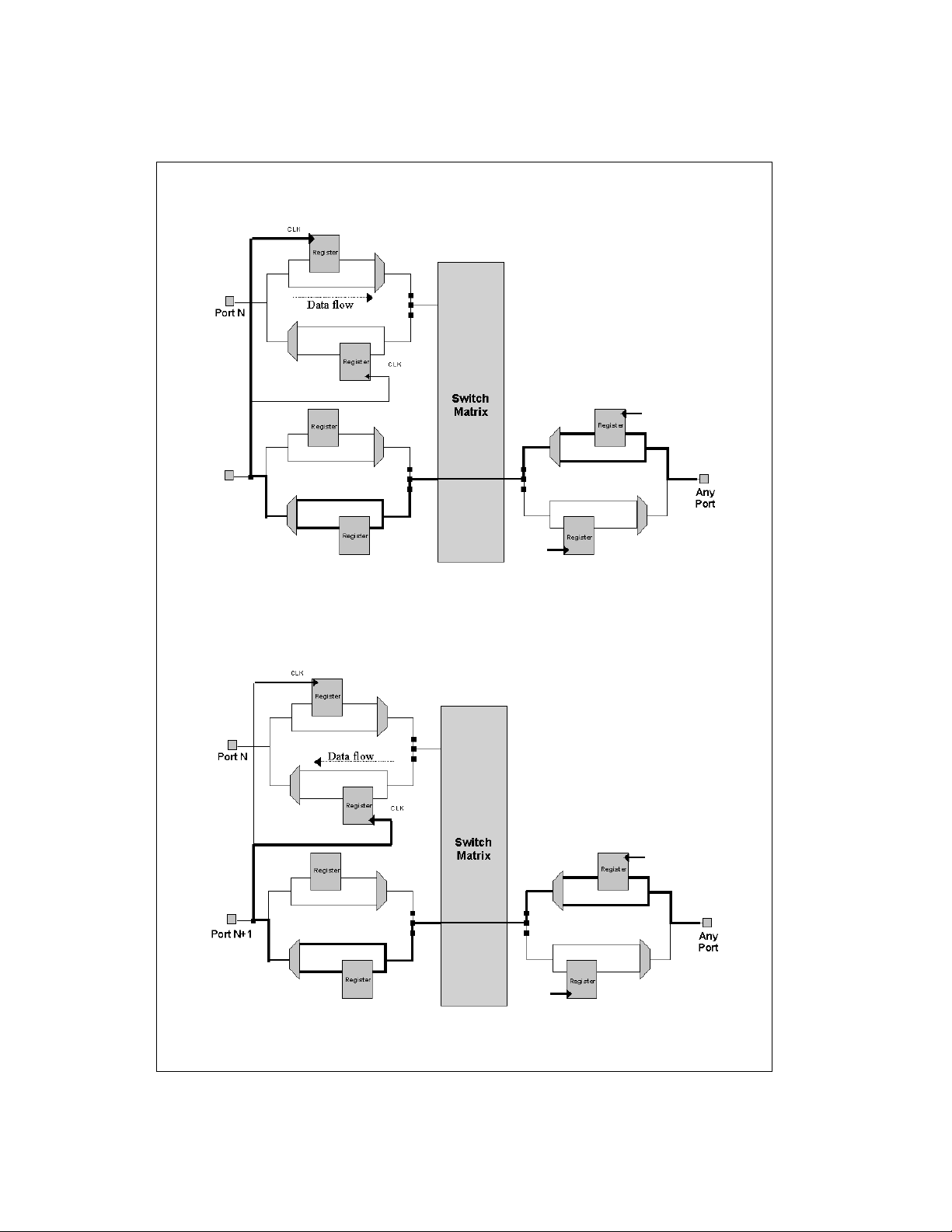
Included among the clocking options in MSX532 is the ability to use an adjacent port as a clock source. This is
referred to as a Next-Neighbor Clock. In the MSX532, Port
0 can be clocked by Port 1, which can be clocked by Port 2,
which can be clocked by Port 3 , etc. In turn, Port 53 1 can
be clocked by Port 0. Since each I/O buffer can be programmed as an input or an outpu t (among other options)
there are four ways to utilize the next neighbor clock
option.
3 www.fairchildsemi.com

Introduction (Continued)
MSX532
Option 1: Registered Input with Next-Neighbor Clock as Input
Option 2: Registered Output with Next-Neighbor Clock as Input
www.fairchildsemi.com 4
Introduction (Continued)
Option 3: Registered Input with Next-Neighbor Clock as Output
MSX532
Option 4: Registered Output with Next-Neighbor Clock as Output
5 www.fairchildsemi.com

Introduction (Continued)
MSX532
Symbol I/O Port Function Mnemonic
TAB LE 1. Summary for Programmable I/O Attributes for MSX Devices
Input The external signal is buffered from the Input Port pin to the
corresponding Switch Matrix line.
IN
Output The internal signal is buffered from the corresponding
Registered
Input
Registered
Output
Bidirectional
Transceiver
Bus
Repeater
Pin Side
Force 0
Switch Matrix line to the Output Port pin. In this mode an
optional output enable (OE
level is logic 0. The output data inversion mode is available
to invert the output signal.
The external signal at the I/O Port is registered into an edgetriggered register within the I/O Port. A clock source is
required in this mode. An input enable (IE) is available but
not required.
The internal signal on the Switch Matrix line is registered by
an edge-triggered register within the I/O Port. A clock source
is required in this mode. An output enable (OE
but not required.
The output data inversion mode is NOT available to invert
the output signal.
In this mode, the I/O buffer acts as a bidirectional transceiver
between the I/O Port pin and the corresponding Switch
Matrix line. This mode requires an input enable (IE) and output enable (OE
The output data inversion mode is available to invert the output signal.
In the Bus Repeater mode, the I/O Port behaves as a wire
(with a non-zero propagation delay). This unique feature
patented by Fairchild incorporates as self-sensing circuit to
determine signal direction and does not require a direction
control signal.
When multiple I/O Ports, configured as “Bus Repeater”, are
connected together through the Switch Matrix to form a single internal node, any (open collector or 3-STA TABLE) LOW
(logic “0”) external signal appearing a t any one of the I/O
Ports gets repeated (or broadcast) to other I/O Ports. For
more details, refer to the Technical Note: “The Bus Repeater
Mode”
In this output mode, the I/O Port pin is forced LOW (logic 0),
regardless of the signal on the corresponding switch Matrix
line. In this mode an optional output enable (OE
selected.
).
) can be selected. The default
) is available
) can be
OP
RI
RO
BT
BR
F0
Pin Side
Force 1
No Connect In this mode, the I/O Port pin is isolated from the Switch
Array Side
Force 0
www.fairchildsemi.com 6
In this output mode, the I/O Port pin is forced HIGH (logic 1),
regardless of the signal on the corresponding Switch Matrix
line. In this mode an optional output enable (OE
selected.
Matrix. This is done by 3-STA TING both the input and output
part of the I/O buffer.
In this input mode, the Switch Matrix line is forced LOW
(logic 0), regardless of the signal on the corresponding I/O
Port. In this mode an optional input enable (IE) can be
selected.
F1
) can be
NC
A0

Introduction (Continued)
DQ
IE
AxPx
CLK
OE
DQ
IE
Ax Px
CLK
OE
D1Q
1
IE
AxPx
CLK_IN
OE
CLK_OP
Q
0D0
Array Side
Force 1
In this input mode, the Switch Matrix line is forced HIGH
(logic 1), regardless of the signal on the corresponding I/O
Port. In this mode an optional input enable (IE) can be
selected.
MSX532
A1
Bidirectional
Transceiver
with
Register
Input
Bidirectional
Transceiver
with
Register
Output
Bidirectional
Transceiver
with
Register I/O
This mode combines Registered Input and buffered Output
(OP). This mode requires a clock source (CLK), and input
enable (IE) and output enable (OE
This mode combines Registered Output (RO) and buffered
Input (IE). This mode requires a clock source (CLK), and
input enable (IE) and output enab le (OE
The output data inversion mode is NOT available to invert
the output signal.
This mode combines Registered Input (RI) and Registered
Output (RO). This mode requires a clock source (CLK), and
input enable (IE) and output enab le (OE
The output data inversion mode is NOT available to invert
the output signal.
).
).
).
BT & RI
BT & RO
BT, RI &
RO
7 www.fairchildsemi.com
Introduction (Continued)
Control Signals
Every port on the MSX devices has two availabl e global
MSX532
clock inputs, input enable s, and output enables. Howeve r,
not all ports have a ccess to the same global control sig nals. There are four global clocks (CLK_0 throug h CLK _3 ),
TABLE 2. M SX Global Control Signals
MSX340 Port
Number
Ports 0-84 Ports 0-132 CLK_0 CLK_1 IE_0 IE_1 OE_0 OE_1
Ports 85-169 Ports 133-265 CLK_1 CLK_2 IE_1 IE_2 OE_1 OE_2
Ports 170-254 Ports 266-398 CLK_2 CLK_3 IE_2 IE_3 OE_2 OE_3
Ports 255-339 Ports 399-531 CLK_3 CLK_0 IE_3 IE_0 OE_3 OE_0
MSX532 Port
Number
Input/Output
Clock Source 1
four global input enables (IE_0 through IE_3), and four global output enables (OE
trol signal is available to half of the ports on the MSX
device. Table 2 below shows the global control sign als that
are available to each port.
Input Output
Clock Source 2
Input
Enable 1
_0 through OE_3). Each global con-
Input
Enable 2
Output
Enable 1
Output
Enable 2
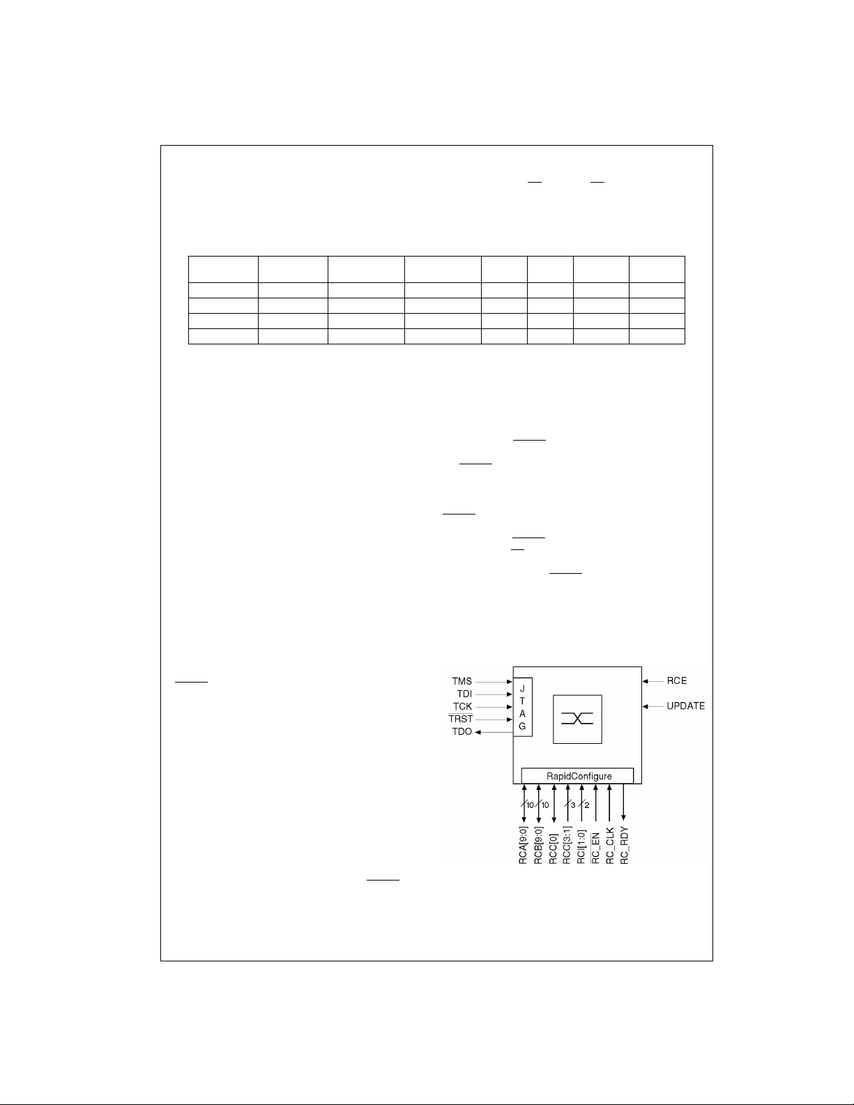
RapidConfigure Interface
The MSX family of Digital Crosspoint Switches can be configured in either of two ways. Both the JTAG serial programming interfac e and the RapidConfigure (RC) par allel
interface can assign crossp oint connectio ns and configure
I/O buffers, but JTAG is a serial input and is slower. JTAG
runs reliably up to 8 MHz and requires over twenty cycles
to program a single command. The RapidConfigur e interface can run at up to 40 MHz a nd can send a new command on every clock cycle. Systems requiring frequent
reconfiguration sh ould be designed to use the RapidC onfigure interface.
RapidConfigure is a 29 signal parall el interface that effectively flattens the serial JTAG bitstream. Rather than con secutively shifting in tw enty or so bits of data to configure
an I/O buffer or make a crosspoint connection, all of these
bits are driven o n the RC lines simultaneously a nd then
latched in by the MSX device in a single cycle. Additionally,
the MSX RapidConf igure interface has b een enhanced to
enable read ing back of configuration data from the device.
RCA[9:0] = RapidConfigure Address A
RCB[9:0]
RCC[3:0]
RCI[1:0]
RC_CLK
RC_EN
RC_RDY
Signal Descriptio n
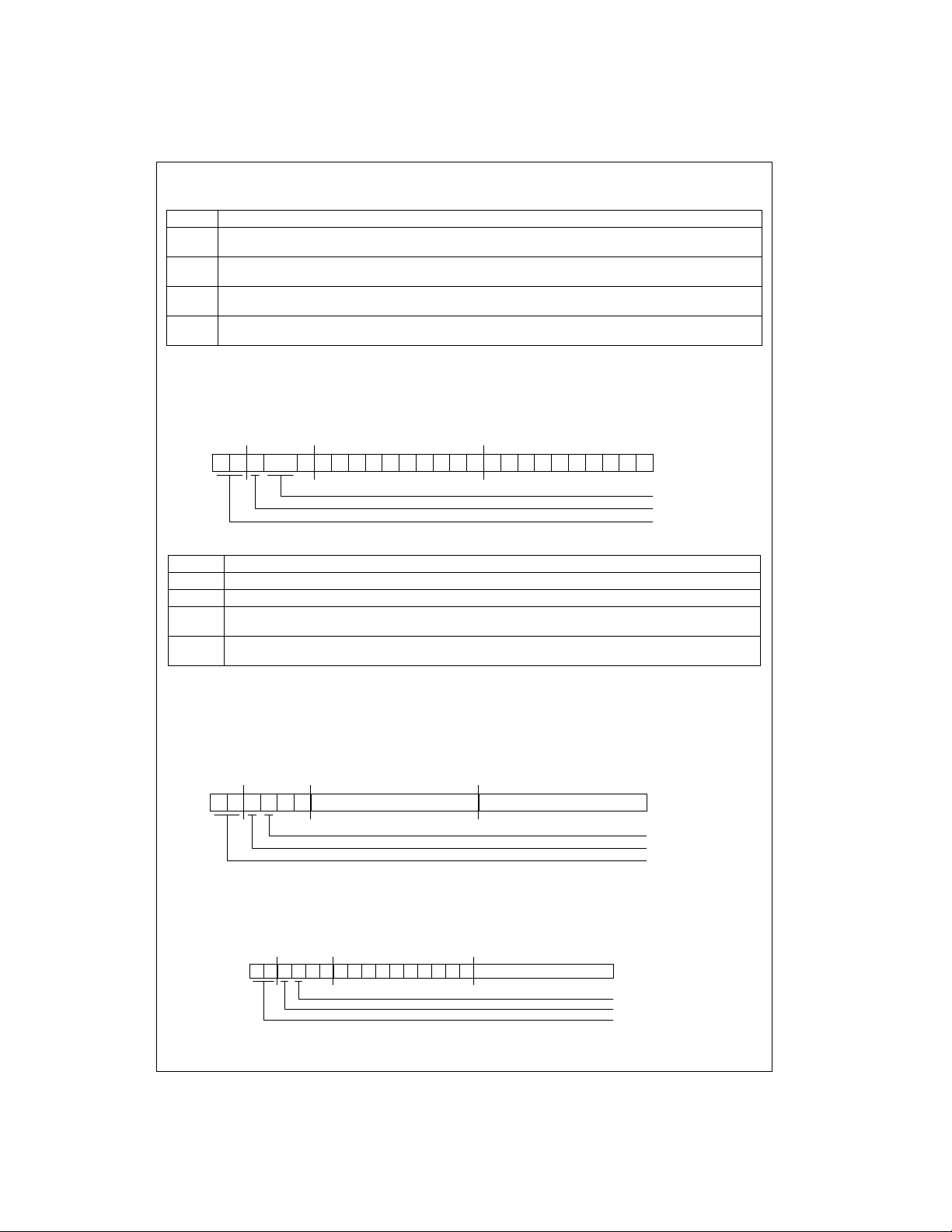
The RC interface su pports four types of operation s. Two
are write operations to the M SX (I/O b uffer configu ra tion or
crosspoint progr amming) an d two are read operatio ns (I/O
buffer and crosspoint configuration read). The RC signals
serve different purp ose s dep ending upon the t ype of o peration being performed.
Most of the signals on th e MSX device’s RC interface are
bi-directional. These signa ls r ec e iv e d ata du r i ng wri t e op erations. During read oper atio ns the se pi ns re ceive data during the first part of the cycle, an d the n drive t he inte rfa ce i n
the final part of the cycle. RCA[9:0], RCB[9:0], and RCC[0]
are bi-directional pins. RCC[3:1], RC_CLK, RC_EN
= RapidConfigure Address B
= RapidConfigure Program Variable C
= RapidConfigure Instruction Bits
= RapidConfigure Clock
= RapidConfigure Cycle Enable
= Read out I/O buffer
and connect/disconnect status
, and
RCI[1:0] are dedicated inputs. RC_RDY is a dedicated output.
The RC_CLK signal is the str obe that latches write data
into the MSX device. I t synchronize s the s ignals driven on
to the RC interface and determines the rate at which commands can be loaded into the MSX device. The MSX
device latches command data on the falling edge of
RC_CLK when RC_EN
can be repeated on consecutive clock s simply by keeping
the RC_EN
on the RCA, RCB, RCC, and RCI signals. RC Read operations require four AC clock cycles and cannot be performed
on back-to-back clocks.
RC_EN
tion. Back-to-back RC Write oper ations may be perf ormed
by keeping the RC_EN
operations RC _EN
complete. Back-to-back RC Read operatio ns can be executed simply by keeping RC_EN
The MSX device as sert s R C_RD Y w h en it has entered the
final stage of a read an d data out is ready. RC_RDY is
asserted on the falling edge of RC_CLK, and de-asserted
on the next falling edge. The MSX device will be driving
valid read data on the RC interface when RC_RDY is
asserted HIGH.
The RC interface specif ies that the RC I sign als b e used to
determine the type of operation being performed.
signal asserted and providing new commands
is an Active LOW signal that enables an RC opera-
FIGURE 4. MSX Switch Configuration Signals
is asserted. RC Write operations
signal asserted. Du ring RC Read
must remain asserted until the cycle is
asserted.
www.fairchildsemi.com 8
Introduction (Continued)
TABLE 3. RapidConfigure Input
RCI [1:0] Description
Force Testing Command. Force commands can force a port to drive either a one or a zero to either the pad or
00
crosspoint array. These commands are generally only used for diagnostic testing.
I/O Buffer Programming Command. These commands are used to configure a port as an input or output,
01
registered or not, etc.
Crosspoint Array Programming Command. Crosspoint connections can be made or broken, or an individual port
10
can be reset.
Read and Reset Commands. This setting is used to read back configuration data from an I/O buffer or crosspoint
11
connection information. It can also be used to reset all of the I/O buffers and the crosspoint array.
Read and Reset Commands
When RCI[1:0] are equal to 11 a Read or Reset command is executed (see Table 4: Reset Commands).
Reset Commands
MSX532
RCI[1:0] RCC[3:0] RCB[9:0] RCA[9:0]
12301
0
789
6
345
2
901
8
567
4
123
0
1 0 0 01 0 0 0 0 0 0 0 0 0 0 0 0 0 0 0 0 0 0 0
Reset Cmd Options
Reset Command
Read/Reset Cmd
TABLE 4. Reset Commands (Continued)
RCC [2:1] Description
00 Reserved. This is not a valid command.
01 Reserved. This is not a valid command.
Crosspoint Array Reset. This command will reset the entire crosspoint array, breaking any previously existing
10
connections.
Crosspoint Array and I/O Buffer Reset. This command resets both the I/O buffers and the crosspoint array as
11
described above.
RCC[0], RCB[9:0], and RCA[9:0] have no function during a reset command and must be written as zeroes.
Crosspoint Read Commands
A crosspoint read is used to check wheth er two ports are
connected through the crosspo int array. The two ports are
addressed using RCA[9:0] and RCB[9:0]
RCI[1:0] RCC[3:0] RCB[9:0] RCA[9:0]
1 11 0 0
12301
0
0
789
6
345
Port #1 Port #2
The MSX device uses RCC[0] to show whether the two
ports are connected. It drives RCC[0] HIGH if the two ports
are connected, and pulls RCC[0] LOW if the two ports are
not connected.
901
2
8
567
4
123
0
Cross Point Read
Read Command
Read/Reset Cmd
I/O Buffer Read Commands
I/O Buffer reads are more comp licated (see Table 5: I/O
Buffer read Commands). The port to be read is addressed
RCI[1:0] RCC[3:0] RCB[9:0] RCA[9:0]
1 11 1 0
12301
0
0
3456789
2
using RCA[9:0]. The MSX device uses RCA[9:0] and
RCB[9:0] to return all o f the config uration data for the p articular I/O buffer.
0
901
567
8
I/O Buffer Address0 0 0 0 0 0 0 0 0 0
123
4
I/O Buffer Config Read
Read Command
Read/Reset Command
9 www.fairchildsemi.com
Introduction (Continued)
TABLE 5. I/O Buffer Read Commands
Signal Description
MSX532
RCA[0] RCA[0] is set to one if the I/O buffer is an input. It is zero if the I/O buffer is not configured as an input. Note that an
RCA[1] RCA[1] is set to a one if the I/O buffer is an output. It is zero if the I/O buffer is not configured as an output. If
RCA[2] RCA[2] is set to a one if the I/O buffer is configured in Bus Repeater Mode. It is zero if the I/O buffer is not in Bus
RCA[3] RCA[3] is set to a one if the I/O buffer is configured as a registered input and is assigned to use its Input Clock 1.
RCA[4] RCA[4] is set to a one if the I/O buffer is configured as a registered input and is assigned to use its Input Clock 2.
RCA[5] RCA[5] is set to a one if the I/O buffer is configured as a registered input and assigned to use Next Neighbor
RCA[6] RCA[6] is set to a one if the I/O buffer is configured as a registered output and is assigned to use its Output Clock
RCA[7] RCA[7] is set to a one if the I/O buffer is configured as a registered output and is assigned to use its Output Clock
I/O buffer can be configured as an Input, Output, Input and Output (in bi-directional mode), or No Connect. All I/O
buffers default to inputs at power-on reset or following a global I/O buffer Reset command, so RCA[0] will read as
a one at reset.
RCA[0] Function
0 I/O buffer not set to input
1 I/O buffer set to input (default)
RCA[1:0] equal 00 the I/O buffer is configured as a No Connect. A No Connect means that the I/O pin of the MSX
device is not connected to the crosspoint array. RCA[1] will read as a zero at reset.
RCA[1] Function
0 I/O buffer not set to output (default)
1 I/O buffer set to output
Repeater Mode. Bus Repeater Mode will be disabled by default at reset, so RCA[2] will read as a zero.
RCA[2] Function
0 I/O buffer not set to Bus Repeater Mode (default)
1 I/O buffer set to Bus Repeater Mode
It is zero if the I/O buffer is not using Input Clock 1. Input Clock 1 for each I/O buffer will vary depending upon the
quadrant of the device in which it resides. RCA[3] will read as a zero at reset.
RCA[3] Function
0 I/O buffer not set to registered input mode (default)
1 I/O buffer set to registered input mode
It is zero if the I/O buffer is not using Input Clock 2. As with Input Clock 1, the source changes depending upon the
quadrant of the device in which the I/O buffer resides. RCA[4] will read as a zero at reset.
RCA[4] Function
0 I/O buffer not using Input Clock Source 2 in RI mode (default)
1 I/O buffer using Input Clock Source 2 in RI mode
Clocking. It is zero if Next Neighbor Clocking is disabled. Next Neighbor Clocking allows the I/O buffer to be registered using the next higher numbered Port number signal as its input clock source. Port 100 on the MSX devices
can use the signal from Port 101 for its input clock if this mode is enabled. Port 531’s Next Neighbor is Port 0. Next
Neighbor Clocking will be disabled by default at reset, so RCA[5] will read as a zero.
RCA[5] Function
0 I/O buffer not using Next Neighbor Clock in RI mode (default)
1 I/O buffer using Next Neighbor Clock in RI mode
1. It is zero if the I/O buffer is not using Output Clock 1. As with Input Clock 1 and 2, the Output Clocks will vary
depending upon the quadrant of the device in which the I/O buffer res ides. In the case of the MSX devices , the
Output Clock 1 and Input Clock 1 for each I/O buffer have the same source, and the Output Clock 2 and Input
Clock 2 do as well. RCA[6] will read as a zero at reset.
RCA[6] Function
0 I/O buffer not using Output Clock Source 1 in RO mode (default)
1 I/O buffer using Output Clock Source 1 in RO mode
2. It is zero if the I/O buffer is not using Output Clock 2. As with Output Clock 1, the source changes depending
upon the quadrant of the device in which the I/O buffer resides. RCA[7] will read as a zero at reset.
RCA[7] Function
0 I/O buffer not using Output Clock Source 2 in RO mode (default)
1 I/O buffer using Output Clock Source 2 in RO mode
I/O Buffer Read Commands (Continued)
www.fairchildsemi.com 10

Introduction (Continued)
Signal Description
RCA[8] RCA[8] is set to a one if the I/O buffer is configured as a registered output and is assigned to use Next Neighbor
RCA[9] RCA[9] is set to a one if the I/O buffer is assigned to use Input Enable 1. It is zero if the I/O buffer is not using Input
RCB[0] RCB[0] is set to a one if the I/O buffer is assigned to use Input Enable 2. It is zero if the I/O buffer is not using Input
RCB[1] RCB[1] is set to a one if the I/O buffer is assigned to use Output Enable 1. It is zero if the I/O buffer is not using
RCB[2] RCB[2] is set to a one if the I/O buffer is assigned to use Output Enable 2. It is zero if the I/O buffer is not using
RCB[6:3] RCB[6:3] are reserved.
RCB[7] RCB[7] is set to a one if the I/O buffer is configured as an inverted output. It is zero if the I/O buffer is not config-
RCB[8] RCB[8] is set to a one if the I/O buffer is configured as a registered input and is using an inverted input clock
RCB[9] RCB[9] is set to a one if the I/O buffer is configured as a registered output and is using an inverted output clock
Clocking. It is zero if Next Neighbor Clocking is disabled. Next Neighbor Clocking allows the I/O buffer to be registered using the next higher numbered Port number signal as its output clock source. Port 100 on the MSX devices
can use the signal from Port 101 for its output clock if this mode is enabled. Port 531’s Next Neighbor is Port 0.
Next Neighbor Clocking will be disabled by default at reset, so RCA[8] will read as a zero.
RCA[8] Function
0 I/O buffer not using Next Neighbor Clock in RO mode (default)
1 I/O buffer using Next Neighbor Clock in RO mode
Enable 1. All bi-directional I/O buffers must use one of the dedicated input enable pins (IE_0, IE_1, IE_2, or IE_3)
to enable the I/O buffer to drive data into the crosspoint array. As with the dedicated clock pins, each I/O buffer can
access two input enable signals, which will vary depending upon the quadrant of this chip in which the I/O buffer
resides. RCA[9] will read as a zero at reset.
RCA[9] Function
0 I/O buffer not using Input Enable Source 1 (default)
1 I/O buffer using Input Enable Source 1
Enable 2. RCB[0] will read as a zero at reset.
RCB[0] Function
0 I/O buffer not using Input Enable Source 2 (default)
1 I/O buffer using Input Enable Source 2
Output Enable 1. All bi-directional I/O buffers must use one of the dedicated output enable pins (OE
_2, or OE_3) to enable the I/O buffer to drive the pin of the device. As with the dedicated clock pins, each I/O
OE
buffer can access two output enable signals, which will vary depending upon the quadrant of the chip in which the
I/O buffer resides. RCB[1] will read as a zero at reset.
RCB[1] Function
0 I/O buffer not using Output Enable Source 1 (default)
1 I/O buffer using Output Enable Source 1
Output Enable 2. RCB[2] will read as a zero at reset.
RCB[2] Function
0 I/O buffer not using Output Enable Source 2 (default)
1 I/O buffer using Output Enable Source 2
ured as an inverted output. The output of any I/O buffer may be inverted so long as it is not a registered output or
running in Bus Repeater Mode. RCB[7] will read as a zero at reset.
RCB[7] Function
0 I/O buffer not configured as inverted output (default)
1 I/O buffer configured as inverted output
source. It is zero if it is not using an inverted input clock. Inputs can use any of the three clock sources described
above and may invert that clock if desired. RCB[8] will read as a zero at reset.
RCB[8] Function
0 I/O buffer not using inverted clock source in RI mode (default)
1 I/O buffer using inverted clock source in RI mode
source. It is zero if it is not using an inverted output clock. Outputs can use any of the three clock sources
described above and may invert that clock if desired. RCB[9] will read as a zero at reset.
RCB[9] Function
0 I/O buffer not using inverted clock source in RO mode (default)
1 I/O buffer using inverted clock source in RO mode
_0, OE_1,
MSX532
11 www.fairchildsemi.com
 Loading...