Fairchild Semiconductor LP2951 Datasheet

www.fairchildsemi.com
LP2951
Adjustable Micro Power Voltage Regulator
Features
• Low Quiescent Current
• Low Dropout Voltage
• Low Temperature Coefficient
• Tight Line and Load Regulat ion
• Guaranteed 100mA Output Current
• Internal Short Current & Thermal Limit
• Error Signals of Output Dropout (8 pin Versions Only)
• External Shut-down ( 8 pin Versions Only)
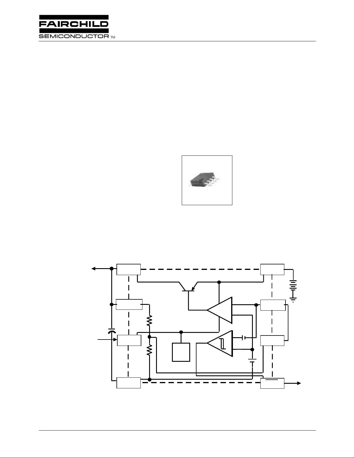
Internal Block Diagram
Description
The LP2951 is an adjustable micro power voltage regulator
suitable for use in battery-powered systems. This regulator
has various functions such as alarm which warns of a low
output voltage, often due to falling batteries on the input, the
external shutdown which enables the regulator to be
switched on and off, current and temperature limiting.
8-SOP
1
PROGRAM
(2)
C1
FROM
EXTERNAL
INPUT
©2001 Fairchild Semiconductor Corporation
SHUTDOWN(3)
GROUND(4)
OUT(1)
SCP
ERROR
AMPLIFIER
ERROR
COMPARATO
COMPARATOR
R
----
++++
++++
----
OFFSE
++++
T
1.25V
REFERENCE
INPUT(8)
FEE DBACK(7)
++++
ERROR(5)
TAP(6)
++++
TO
EXTERNAL
INPUT
Rev. 1.0.0

LP2951
Absolute Maximum Ratings
Parameter Symbol Value Unit
Input Supply Voltage V
Power Dissipation P
Thermal Resistance Junction-Air R
Storage Temperature Range T
Operating Junction Temperature Range T
IN
D
θJA
STG
OPR
-0.3 ~ +30 V
Internally Limited W
127.5 °C/W
-65 ~ +150 °C
-40 ~ +125 °C
2

Electrical Characteristics
(Refer to the test circuit, Ta = 25 °C, unless otherwise specified, )
Parameter Symbol Conditions Min. Typ. Max. Unit
ALL VOLTAGE OPTIONS
Output Voltage Temperature Coefficient ∆V
Line Regulation (Note2) ∆V
Load Regulation (Note2) ∆V 100uA≤ I
Dropout Voltage V
Ground Current I
Current Limit I
8-PIN VERSIONS ONLY
Reference Voltage
ERROR COMPARATOR
Output Low Voltage V
High Threshold Voltage V
Low Threshold Voltage V
Hysteresis V
SHUTDOWN INPUT
Shutdown Threshold Range V
Shutdown Input Current I
∆T (Note1) - 50 - ppm/°C
/
(Vo + 1)V≤V
= 50mA
I
L
IL = 100uA - - 150 mV
D
= 100mA - - 600 mV
I
L
IL = 100uA - - 140 uA
V
V
G
CL
REF
REF
OL
TH
TL
HYS
SD
= 100mA - - 7 mA
I
L
VO = 0V 110 165 220 mA
(Note3)
VIN = (Vo - 0.5)V, I
(Note4) 25 60 - mV
(Note4) - 75 140 mV
(Note4) - 15 - mV
(Note5) 0.6 1.3 2.0 V
VSD = 2.4V - 30 100 uA
SD
= 28V - 450 750 uA
V
SD
≤28V
IN
≤100mA - - 0.3 %
L
--0.4%
1.235 1.26 1.285 V
1.225 1.26 1.295 V
=400uA - 150 400 mV
OL
LP2951
Note :
1. Output or reference voltage temperature coefficient is defined as the worst case voltage change divided by the total
temperature range.
2. Regulation is measured at constant junction temperature , using pulse testing with a low duty cycle.
3. V
≤ V
ref
out
4. Threshold and hysteresis are expressed in terms of voltage differential at the Feedback terminal below the normal
reference . To express these thresholds in terms of output voltage change , multiply by the error amplifier gain
= VO / VREF = (R1 + R2) / R2 .
5. Vshutdown ≤ 0.6 V , V
- 1V), 2.5V ≤ Vin ≤ 28V, 100uA ≤ IL ≤ 100mA, TA ≤ T
≤ (V
in
=ON , Vshutdown ≥ 2.0 V, V
OUT
OUT
= OFF.
AMAX
.
3
 Loading...