

Fairchild Semiconductor HUFA76413DK8 Datasheet
©2003 Fairchild Semiconductor Corporation
January 2003
Rev. B
HUFA76413DK8T
HUFA76413DK8T
N-Channel Logic Level UltraFET® Power MOSFET
60V, 4.8A, 56m Ω
General Description
These N-Channel power MOSFETs are manufactured using the innovative UltraFET
®
process. This advanced process technology achieves the lowest possible onresistance per silicon area, resulting in outstanding performance. This device is capable of withstanding high energy
in the avalanche mode and the diode exhibits very low reverse recovery time and stored charge. It was designed for
use in applications where power efficiency is important,
such as switching regulators, switching convertors, mot or
drivers, relay drivers, low-voltage bus switches, and power
management in portable and battery-operated products.
Applications
• Motor and Load Control
• Powertrain Management
Features
• 150°C Maximum Junction Temperature
• UIS Capability (Single Pulse and Repetitive Pulse)
• Ultra-Low On-Resistance r
DS(ON)
= 0.049Ω, VGS = 10V
• Ultra-Low On-Resistance r
DS(ON)
= 0.056Ω, VGS = 5V
MOSFET Maximum Ratings T
A
= 25°C unless otherwise noted
Thermal Characteristics
This product has been designed to meet the extreme test conditions and environment demanded by the automotive industry. For a
copy of the requirements, see AEC Q101 at: http://www.aecouncil.com/
Reliability data can be found at: http://www.fairchildsemi.com/products/discrete/reliability/index.html.
All Fairchild Semiconductor products are manufactured, assembled and tested under ISO9000 and QS9000 quality systems
certification.
Symbol Parameter Ratings Units
V
DSS
Drain to Source Voltage 60 V
V
GS
Gate to Source Voltage ±16 V
I
D
Drain Current
5.1 A
Continuous (T
C
= 25oC, VGS = 10V)
Continuous (T
C
= 25oC, VGS = 5V) 4.8 A
Continuous (T
C
= 125oC, VGS = 5V, R
θJA
= 228oC/W) 1 A
Pulsed Figure 4 A
E
AS
Single Pulse Avalanche Energy (Note 1) 260 mJ
P
D
Power dissipation 2.5 W
Derate above 25
o
C0.02W/
o
C
T
J
, T
STG
Operating and Storage Temperature -55 to 150
o
C
R
θJA
Thermal Resistance Junction to Ambient SO-8 (Note 2) 50
o
C/W
R
θJA
Thermal Resistance Junction to Ambient SO-8 (Note 3) 191
o
C/W
R
θJA
Thermal Resistance Junction to Ambient SO-8 (Note 4) 228
o
C/W
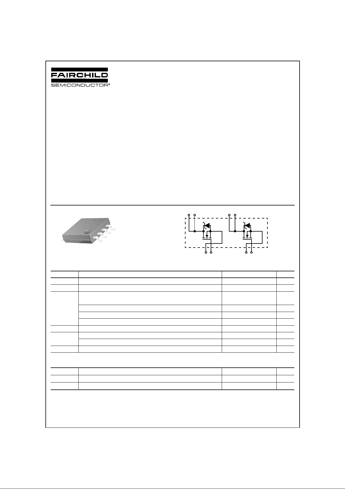
G1 (2)
D1 (8)
S1 (1)
D1 (7)
D2 (6) D2 (5)
S2 (3) G2 (4)
SO-8
1
©2003 Fairchild Semiconductor Corporation Rev. B
HUFA76413DK8T
Package Marking and Ordering Information
Electrical Characteristics T
A
= 25°C unless otherwise noted
Off Characteristics
On Characteristics
Dynamic Characteristics
Switching Characteristics
(VGS = 5V)
Drain-Source Diode Characteristics
Notes:
1: Starting TJ = 25°C, L = 20mH, IAS = 5.1A
2: R
θJA
is 50 oC/W when mounted on a 0.5 in2 copper pad on FR-4 at 1 second.
3: R
θJA
is 191 oC/W when mounted on a 0.027 in2 copper pad on FR-4 at 1000 seconds.
4: R
θJA
is 228 oC/W when mounted on a 0.006 in2 copper pad on FR-4 at 1000 seconds.
Device Marking Device Package Reel Size Tape Width Quantity
76413DK8 HUFA76413DK8T SO-8 330mm 12mm 2500 units
Symbol Parameter Test Conditions Min Typ Max Units
B
VDSS
Drain to Source Breakdown Voltage ID = 250µA, VGS = 0V 60 - - V
I
DSS
Zero Gate Voltage Drain Current
V
DS
= 50V - - 1
µA
V
GS
= 0V TA = 150oC - - 250
I
GSS
Gate to Source Leakage Current VGS = ±16V - - ±100 nA
V
GS(TH)
Gate to Source Threshold Voltage VGS = VDS, ID = 250µA1-3V
r
DS(ON)
Drain to Source On Resistance
I
D
= 5.1A, VGS = 10V - 0.041 0. 049
Ω
I
D
= 4.8A, VGS = 5V - 0.048 0. 056
I
D
= 4.8A, VGS = 5V
T
A
= 150oC
- 0.091 0.106
C
ISS
Input Capacitance
V
DS
= 25V, VGS = 0V,
f = 1MHz
- 620 - pF
C
OSS
Output Capacitance - 180 - pF
C
RSS
Reverse Transfer Capacitance - 30 - pF
Q
g(TOT)
Total Gate Charge at 10V VGS = 0V to 10V
V
DD
= 30V
I
D
= 4.8A
I
g
= 1.0mA
18 23 nC
Q
g(5)
Total Gate Charge at 5V VGS = 0V to 5V - 10 13 nC
Q
g(TH)
Threshold Gate Charge VGS = 0V to 1V - 0.6 0.8 nC
Q
gs
Gate to Source Gate Charge - 1.8 - nC
Q
gd
Gate to Drain “Miller” Charge - 5 - nC
t
ON
Turn-On Time
V
DD
= 30V, ID = 1A
V
GS
= 5V, RGS = 16Ω
- - 44 ns
t
d(ON)
Turn-On Delay Time - 10 - ns
t
r
Rise Time - 19 - ns
t
d(OFF)
Turn-Off Delay Time - 45 - ns
t
f
Fall Time - 27 - ns
t
OFF
Turn-Off Time - - 108 ns
V
SD
Source to Drain Diode Voltage
I
SD
= 4.8A - - 1.25 V
I
SD
= 2.4A - - 1.0 V
t
rr
Reverse Recovery Time ISD = 4.8A, dISD/dt = 100A/µs- - 43 ns
Q
RR
Reverse Recovered Charge ISD = 4.8A, dISD/dt = 100A/µs- - 55 nC
©2003 Fairchild Semiconductor Corporation Rev. B
HUFA76413DK8T
Typical Characteristics T
A
= 25°C unless otherwise noted
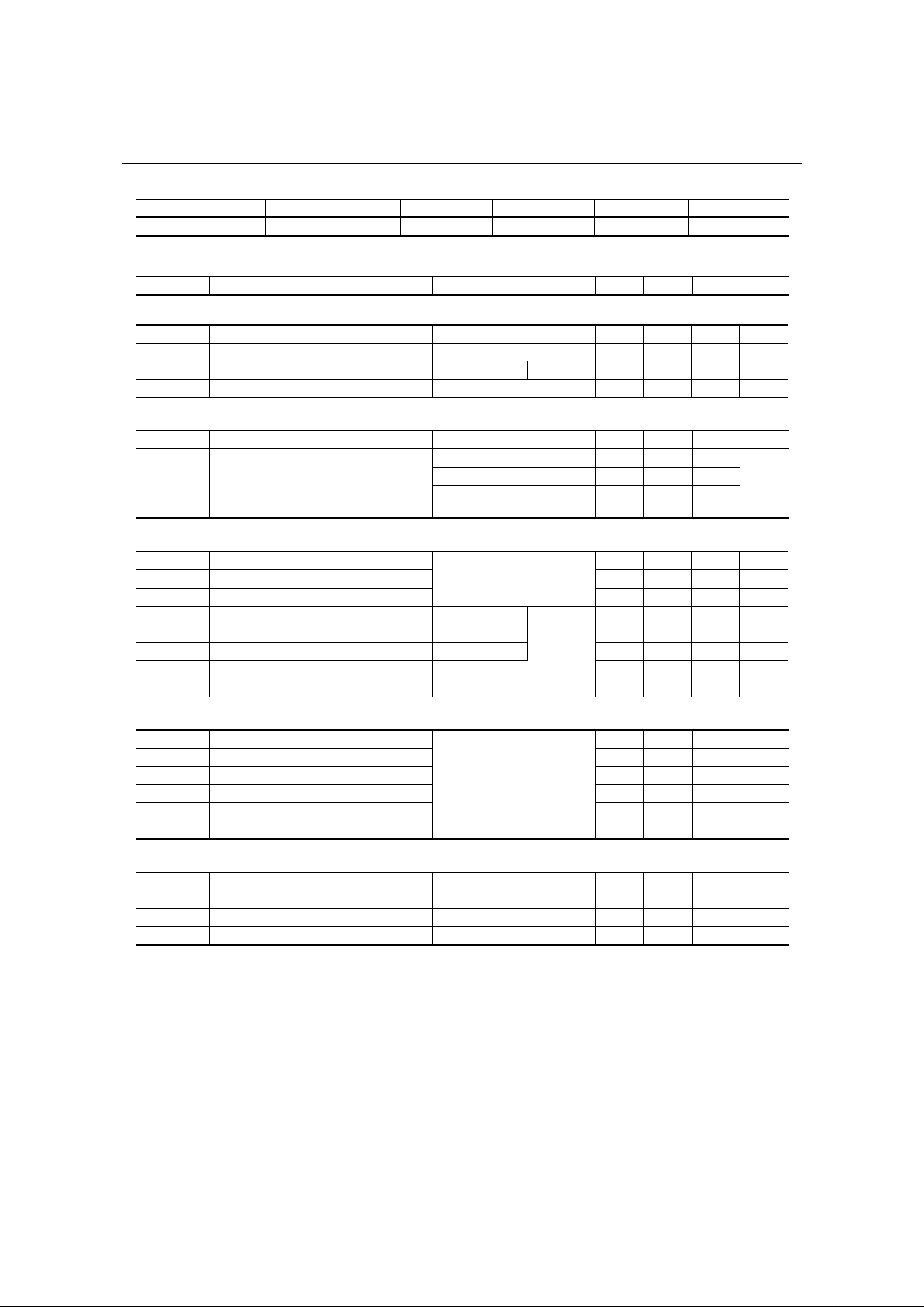
Figure 1. Normalized Power Dissipation vs
Ambient Temperature
Figure 2. Maximum Contin uous Drain Current vs
Case Temperature
Figure 3. Normalized Maximum Transient Thermal Impedance
Figure 4. Peak Current Capability
TA, AMBIENT TEMPERATURE (oC)
POWER DISSIPATION MULTIPLIER
0
0 25 50 75 100 150
0.2
0.4
0.6
0.8
1.0
1.2
125
0
2
4
6
25 50 75 100 125 150
-I
D
, DRAIN CURRENT (A)
TA, CASE TEMPERATURE (oC)
V
GS
= 10V, R
θJA
=50oC/W
V
GS
= 5V, R
θJA
=228oC/W
0.001
0.01
0.1
1
10
-4
10
-3
10
-2
10
-1
10
0
10
1
10
2
10
3
4
10
-5
t, RECTANGULAR PULSE DURATION (s)
Z
θJA
, NORMALIZED
THERMAL IMPEDANCE
NOTES:
DUTY FACTOR: D = t1/t
2
PEAK TJ = PDM x Z
θJA
x R
θJA
+ T
A
P
DM
t
1
t
2
0.5
0.2
0.1
0.05
0.01
0.02
DUTY CYCLE - DESCENDING ORDER
SINGLE PULSE
VGS = 10V
R
θJA
=50oC/W
10
100
300
2
10
-5
10
-3
10
-4
10
-2
10
-1
10
0
10
1
10
2
10
3
I
DM
, PEAK CURRENT (A)
t, PULSE WIDTH (s)
TRANSCONDUCTANCE
MAY LIMIT CURRENT
IN THIS REGION
VGS = 5V
TA = 25oC
I = I
25
175 - T
A
150
FOR TEMPERATURES
ABOVE 25oC DERATE PEAK
CURRENT AS FOLLOWS:
VGS = 10V
R
θJA
=50oC/W
©2003 Fairchild Semiconductor Corporation Rev. B
HUFA76413DK8T
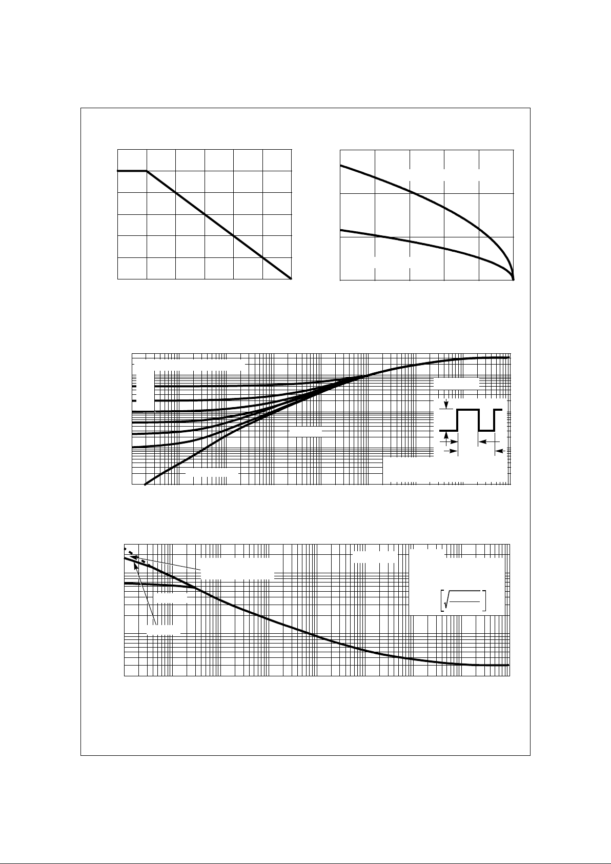
Figure 5. Forward Bias Safe Operating Area Figure 6. Unclamped Inductive Switching
Capability
Figure 7. Transfer Ch aracteri stics Figure 8. Saturation Character istics
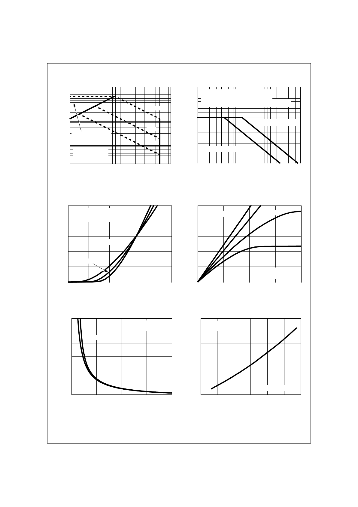
Figure 9. Drain to Source On Resis tanc e vs Ga te
Voltage and Drain Current
Figure 10. Normalized Drain to Source On
Resistance vs Junction Temperature
Typical Characteristics T
A
= 25°C unless otherwise noted
1
10
100
110100
0.2
200
VDS, DRAIN TO SOURCE VOLTAGE (V)
I
D
, DRAIN CURRENT (A)
TJ = MAX RATED
TA = 25oC
SINGLE PULSE
LIMITED BY r
DS(ON)
AREA MAY BE
OPERATION IN THIS
100µs
10ms
1ms
1
10
0.1 1 10
15
40
I
AS
, AVALANCHE CURRENT (A)
tAV, TIME IN AVALANCHE (ms)
STARTING TJ = 25oC
STARTING TJ = 150oC
tAV = (L)(IAS)/(1.3*RATED BV
DSS
- VDD)
If R = 0
If R ≠ 0
tAV = (L/R)ln[(IAS*R)/(1.3*RATED BV
DSS
- VDD) +1]
0
5
10
15
20
25
1.5 2.0 2.5 3.0 3.5 4.0
I
D
, DRAIN CURRENT (A)
VGS, GATE TO SOURCE VOLTAGE (V)
PULSE DURATION = 80µs
DUTY CYCLE = 0.5% MAX
V
DD
= 15V
TJ = 150oC
TJ = 25oC
TJ = -55oC
0
5
10
15
20
25
0 0.5 1.0 1.5 2.0
I
D
, DRAIN CURRENT (A)
VDS, DRAIN TO SOURCE VOLTAGE (V)
VGS = 3.5V
PULSE DURATION = 80µs
DUTY CYCLE = 0.5% MAX
VGS = 3V
TA = 25oC
VGS = 5V
VGS = 10V
40
50
60
70
80
90
100
246810
ID = 1A
VGS, GATE TO SOURCE VOLTAGE (V)
ID = 5.1A
r
DS(ON)
, DRAIN TO SOURCE
ON RESISTANCE (mΩ)
PULSE DURATION = 80µs
DUTY CYCLE = 0.5% MAX
0.5
1.0
1.5
2.0
-80 -40 0 40 80 120 160
NORMALIZED DRAIN TO SOURCE
TJ, JUNCTION TEMPERATURE (oC)
ON RESISTANCE
VGS = 10V, ID =5.1A
PULSE DURATION = 80µs
DUTY CYCLE = 0.5% MAX
 Loading...