

Fairchild Semiconductor HUFA75631SK8 Datasheet
Data Sheet December 2001
5.5A, 100V, 0.039 Ohm, N-Channel,
UltraFET® Power MOSFET
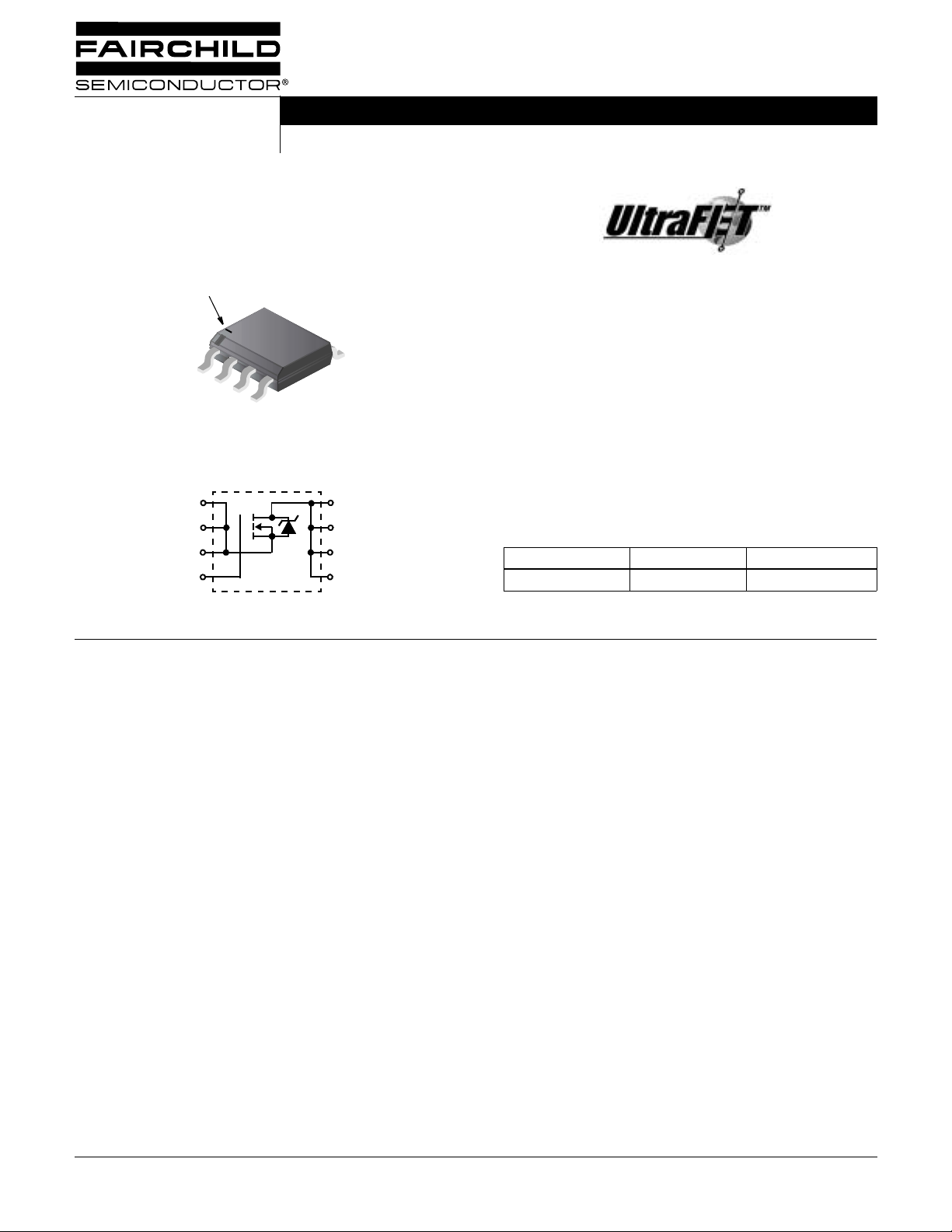
Packaging
JEDEC MS-012AA
BRANDING DASH
5
1
2
3
4
Symbol
HUFA75631SK8
Features
• Ultra Low On-Resistance
-r
DS(ON)
= 0.039Ω,
• Simulation Models
- Temperature Compensated PSPICE® and SABER™
Electrical Models
- Spice and SABER Thermal Impedance Models
- www.fairchildsemi.com
• Peak Cu rrent vs Pulse Width Curve
V
= 10V
GS
SOURCE (1)
SOURCE (2)
SOURCE (3)
GATE (4)
Absolute Maximum Ratings
Drain to Source Voltage (Note 1). . . . . . . . . . . . . . . . . . . . . . . . . . . . . . . . . . . . . . . . . . . . . . . V
Drain to Gate Voltage (R
Gate to Source Voltage . . . . . . . . . . . . . . . . . . . . . . . . . . . . . . . . . . . . . . . . . . . . . . . . . . . . . . . V
Drain Current
Continuous (T
Continuous (TA = 100oC, VGS = 10V) (Figure 2) . . . . . . . . . . . . . . . . . . . . . . . . . . . . . . . . . . I
Pulsed Drain Current . . . . . . . . . . . . . . . . . . . . . . . . . . . . . . . . . . . . . . . . . . . . . . . . . . . . . . . . I
Pulsed Avalanche Rating . . . . . . . . . . . . . . . . . . . . . . . . . . . . . . . . . . . . . . . . . . . . . . . . . . . . . . UIS Figures 6, 14, 15
Power Dissipation . . . . . . . . . . . . . . . . . . . . . . . . . . . . . . . . . . . . . . . . . . . . . . . . . . . . . . . . . . . . P
Derate Above 25oC . . . . . . . . . . . . . . . . . . . . . . . . . . . . . . . . . . . . . . . . . . . . . . . . . . . . . . . . . . . .
Operating and Storage Temperature . . . . . . . . . . . . . . . . . . . . . . . . . . . . . . . . . . . . . . . . . T
Maximum Temperature for Soldering
Leads at 0.063in (1.6mm) from Case for 10s. . . . . . . . . . . . . . . . . . . . . . . . . . . . . . . . . . . . . . . T
Package Body for 10s, See Techbrief TB334. . . . . . . . . . . . . . . . . . . . . . . . . . . . . . . . . . . . . T
NOTES:
= 25oC to 150oC.
1. T
J
o
C/W measured using FR-4 board with 0.76 in2 (490.3 mm2) copper pad at 10 second.
2. 50
o
3. 152
C/W measured using FR-4 board with 0.054 in2 (34.8 mm2) copper pad at 1000 seconds
o
C/W measured using FR-4 board with 0.0115 in2 (7.42 mm2) copper pad at 1000 seconds
4. 189
CAUTION: Stresses above those listed in “ Absolute M aximum Ratings” may cause perm anent damage to th e device. This is a stress onl y rating and operation of the
device at these or any other conditions above those indicated in the operational sections of this specification is not implied.
A
= 20kΩ) (Note 1) . . . . . . . . . . . . . . . . . . . . . . . . . . . . . . . . . . . . . V
GS
= 25oC, VGS = 10V) (Figure 2) . . . . . . . . . . . . . . . . . . . . . . . . . . . . . . . . . . . I
DRAIN (8)
DRAIN (7)
DRAIN (6)
DRAIN (5)
TA = 25oC, Unless Otherwise Specified
Ordering Information
PART NUMBER PACKAGE BRAND
HUFA75631SK8 MS-012AA 75631SK8
NOTE: When ordering, use the entire part number. Add the suffix T
to obtain the variant in tape and reel, e.g., HUFA75631SK8T.
HUFA75631SK8 UNITS
DSS
DGR
GS
D
D
DM
D
, T
J
STG
L
pkg
100 V
100 V
±20 V
5.5
3.5
Figure 4
2.5
20
-55 to 150
300
260
A
A
W
mW/oC
o
C
o
C
o
C
• UIS Rating Curve
This product has be en desi gned t o mee t t he ex tre me test con diti ons a nd e nviro nment dema nded by the autom otive indu str y. Fo r a copy
Reliability data can be found at: http://www.fairchildsemi.com/products/discrete/reliability/index.html.
All Fairchild semiconductor products are manufactured, assembled and tested under ISO9000 and QS9000 quality systems certification.
©2001 Fairchild Semiconductor Corpo ration HUFA75631SK8 Rev. B
of the requirements, see AEC Q101 at: http://www.aecouncil.com/
HUFA75631SK8
Electrical Specifications
TA = 25oC, Unless Otherwise Specified
PARAMETER SYMBOL TEST CONDITIONS MIN TYP MAX UNITS
OFF STATE SPECIFICATIONS
Drain to Source Breakdown Voltage BV
Zero Gate Voltage Drain Current I
Gate to Source Leakage Current I
ON STATE SPECIFICATIONS
Gate to Source Threshold Voltage V
Drain to Source On Resistance r
THERMAL SPECIFICATIONS
Thermal Resistance Junction to
Ambient
SWITCHING SPECIFICATIONS
Turn-On Time t
Turn-On Delay Time t
Rise Time t
Turn-Off Delay Time t
Fall Time t
Turn-Off Time t
GATE CHARGE SPECIFICATIONS
Total Gate Charge Q
Gate Charge at 10V Q
Threshold Gate Charge Q
Gate to Source Gate Charge Q
Gate to Drain “Miller” Charge Q
CAPACITANCE SPECIFICATIONS
Input Capacitance C
Output Capacitance C
Reverse Transfer Capacitance C
DSSID
DSS
VDS = 95V, VGS = 0V - - 1 µA
V
GSS
GS(TH)VGS
DS(ON)ID
R
θJA
VGS = ±20V - - ±100 nA
Pad Area = 0.76 in2 (490.3 mm2) (Note 2)
(Figures 20, 21)
Pad Area = 0.054 in
(Figures 20, 21)
Pad Area = 0.0115 in
(Figures 20, 21)
ON
VDD = 50V, ID = 5.5A
V
d(ON)
d(OFF)
OFF
g(TOT)VGS
g(10)
g(TH)
ISS
OSS
RSS
(Figures 18, 19)
r
f
VGS = 0V to 10V - 35 43 nC
VGS = 0V to 2V - 2.4 2.9 nC
gs
gd
VDS = 25V, VGS = 0V, f = 1MHz
(Figure 12)
= 250µA, VGS = 0V (Figure 11) 100 - - V
= 90V, VGS = 0V, TA = 150oC - - 250 µA
DS
= VDS, ID = 250µA (Figure 10) 2 - 4 V
= 5.5A, VGS = 10V (Figure 9) - 0.033 0.039 Ω
--50oC/W
2
(34.8 mm2) (Note 3)
2
(7.42 mm2)(Note 4)
- - 152
- - 189
o
o
- - 50 ns
= 10V, RGS = 6.8Ω
GS
-11-ns
-23-ns
-39-ns
-31-ns
- - 105 ns
= 0V to 20V VDD = 50V, ID = 5.5A,
= 1.0mA
I
g(REF)
-6679nC
(Figures 13, 16, 17)
-4.75- nC
-12-nC
- 1225 - pF
- 330 - pF
- 105 - pF
C/W
C/W
Source to Drain Diode Specifications
PARAMETER SYMBOL TEST CONDITIONS MIN TYP MAX UNITS
Source to Drain Diode Voltage V
SD
Reverse Recovery Time t
Reverse Recovered Charge Q
©2001 Fairchild Semiconductor Corpo ration HUFA75631SK8 Rev. B
RR
ISD = 5.5 A - - 1.25 V
I
= 2.5 A - - 1.00 V
SD
ISD = 5.5 A, dISD/dt = 100A/µs--96ns
rr
ISD = 5.5 A, dISD/dt = 100A/µs - - 310 nC
Typical Performance Curves
0
HUFA75631SK8
1.2
1.0
0.8
0.6
0.4
0.2
POWER DISSIPATION MULTIPLIER
0
0255075100 15
125
TA, AMBIENT TEMPERATURE (oC)
FIGURE 1. NORMALIZED POWER DISSIPATION vs AMBIENT
TEMPERATURE
10
DUTY CYCLE - DESCENDING ORDER
0.5
0.2
0.1
1
0.05
0.02
0.01
0.1
, NORMALIZED
θJA
Z
0.01
THERMAL IMPEDANCE
SINGLE PULSE
0.001
-5
10
-4
10
-3
10
-2
10
t, RECTANGULAR PULSE DURATION (s)
6
V
GS
= 10V, R
θ
JA
= 50oC/W
5
4
3
2
, DRAIN CURRENT (A)
D
I
1
0
25
50 75 100 125
TA, AMBIENT TEMPERATURE (oC)
FIGURE 2. MAXIMUM CONTINUOUS DRAIN CURRENT vs
AMBIENT TEMPERATURE
R
= 50oC/W
θJA
P
DM
t
1
t
x R
2
+ T
θJA
A
2
10
NOTES:
DUTY FACTOR: D = t
PEAK TJ = PDM x Z
-1
10
0
10
1
10
1/t2
θJA
150
3
10
FIGURE 3. NORMALIZED MAXIMUM TRANSIENT THERMAL IMPEDANCE
500
100
10
, PEAK CURRENT (A)
TRANSCONDUCTANCE
DM
I
MAY LIMIT CURRENT
IN THIS REGION
1
-5
10
VGS = 10V
-4
10
R
= 50oC/W
θ
JA
-3
10
-2
10
-1
10
0
10
t, PULSE WIDTH (s)
TA = 25oC
FOR TEMPERATURES
ABOVE 25
o
C DERATE PEAK
CURRENT AS FOLLOWS:
I = I
25
1
10
150 - T
10
125
2
A
10
FIGURE 4. PEAK CURRENT CAPABILITY
©2001 Fairchild Semiconductor Corpo ration HUFA75631SK8 Rev. B
3
0
0
6
4
0
HUFA75631SK8
Typical Performance Curves
200
100
10
OPERATION IN THIS
AREA MAY BE
1
, DRAIN CURRENT (A)
D
LIMITED BY r
I
0.1
1
DS(ON)
, DRAIN TO SOURCE VOLTAGE (V)
V
DS
SINGLE PULSE
TJ = MAX RATED
= 25oC
T
A
10 20
(Continued)
R
FIGURE 5. FORWARD BIAS SAFE OPERATING AREA
50
PULSE DURATION = 80µs
DUTY CYCLE = 0.5% MAX
= 15V
V
DD
40
θJA
= 50oC/W
100µs
1ms
10ms
100
100
10
, AVALANCHE CURRENT (A)
AS
I
1
0.01 0.1 1 10
If R = 0
tAV = (L)(IAS)/(1.3*RATED BV
If R ≠ 0
= (L/R)ln[(IAS*R)/(1.3*RATED BV
t
AV
STARTING TJ = 150oC
tAV, TIME IN AVALANCHE (ms)
- VDD)
DSS
- VDD) +1]
DSS
STARTING TJ = 25oC
10
NOTE: Refer to Fairchild Application Notes AN9321 and AN9322.
FIGURE 6. UNCLAMPED INDUCTIVE SWITCHING
CAPABILITY
50
40
VGS = 20V
= 10V
V
GS
VGS = 7V
V
= 6V
GS
30
20
20
DRAIN CURRENT (A)
D,
I
10
0
2345
TJ = 150oC
VGS, GATE TO SOURCE VOLTAGE (V)
TJ = 25oC
TJ = -55oC
30
20
, DRAIN CURRENT (A)
D
I
10
0
0123
VDS, DRAIN TO SOURCE VOLTAGE (V)
PULSE DURATION = 80µs
DUTY CYCLE = 0.5% MAX
T
FIGURE 7. TRANSFER CHARACTERISTICS FIGURE 8. SA TURATION CHARACTERISTICS
2.5
PULSE DURATION = 80µs
DUTY CYCLE = 0.5% MAX
2.0
1.5
ON RESISTANCE
1.0
NORMALIZED DRAIN TO SOURCE
0.5
-80 -40 0 40 80 120 16
TJ, JUNCTION TEMPERATURE (oC)
VGS = 10V, ID = 5.5A
1.2
1.0
0.8
NORMALIZED GATE
THRESHOLD VOLTAGE
0.6
-80 -40 0 40 80 120 160
TJ, JUNCTION TEMPERATURE (oC)
VGS =5V
= 25oC
A
VGS = VDS, ID = 250µA
FIGURE 9. NORMALIZED DRAIN TO SOURCE ON
RESISTANCE vs JUNCTION TEMPERATURE
©2001 Fairchild Semiconductor Corpo ration HUFA75631SK8 Rev. B
FIGURE 10. NORMALIZED GA TE THRESHOLD VOLTA GE vs
JUNCTION TEMPERATURE
 Loading...